CSD16413Q5A
www.ti.com
SLPS199A – AUGUST 2009 – REVISED APRIL 2010
N-Channel NexFET™ Power MOSFET
Check for Samples: C...
CSD16413Q5A
www.ti.com
SLPS199A – AUGUST 2009 – REVISED APRIL 2010
N-Channel NexFET™ Power
MOSFET
Check for Samples: CSD16413Q5A
FEATURES
1
2 Ultra Low Qg and Qgd Low Thermal Resistance Avalanche Rated Pb Free Terminal Plating RoHS Compliant Halogen Free SON 5mm × 6mm Plastic Package
APPLICATIONS
Point-of-Load Synchronous Buck Converter for Applications in Networking, Telecom and Computing Systems
Optimized for Control or Synchronous FET Applications
DESCRIPTION
The NexFET™ power
MOSFET has been designed to minimize losses in power conversion applications.
Top View
S1
8D
S2
7D
S3
D G4
6D
5D
P0093-01
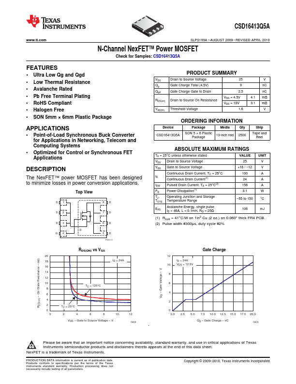
VDS Qg Qgd
RDS(on)
VGS(th)
PRODUCT SUMMARY
Drain to Source
Voltage
25
Gate Charge Total (4.5V)
9
Gate Charge Gate to Drain
2.5
Drain to Source On Resistance Threshold
Voltage
VGS = 4.5V VGS = 10V
1.6
V nC nC 4.1 mΩ 3.1 mΩ V
ORDERING INFORMATION
Device
Package
Media
Qty
CSD16413Q5A
SON 5 × 6 Plastic Package
13-inch reel
2500
Ship
Tape and Reel
ABSOLUTE MAXIMUM RATINGS
TA = 25°C unless otherwise stated
VDS Drain to Source
Voltage
VGS Gate to Source
Voltage
ID
Continuous Drain Current, TC = 25°C Continuous Drain Current(1)
IDM Pulsed Drain Current, TA = 25°C(2)
PD
Power Dissipation(1)
TJ, Operating Junction and Storage TSTG Temperature Range
EAS
Avalanche Energy, single pulse ID = 46A, L = 0.1mH, RG = 25Ω
VALUE 25
+16 / –12 100 24 156 3.1
UNIT V V A A A W
–55 to 150 °C
106
mJ
(1) RqJA = 41°C/W on 1in2 Cu (2 oz.) on 0....