Product Folder
Sample & Buy
Technical Documents
Tools & Software
Support & Community
Reference Design
CSD18503Q5A
...
Product Folder
Sample & Buy
Technical Documents
Tools & Software
Support & Community
Reference Design
CSD18503Q5A
SLPS358C – JUNE 2012 – REVISED JUNE 2015
CSD18503Q5A 40 V N-Channel NexFET™ Power
MOSFET
1 Features
1 Ultra-Low Qg and Qgd Low Thermal Resistance Avalanche Rated Logic Level Pb Free Terminal Plating RoHS Compliant Halogen Free SON 5 mm × 6 mm Plastic Package
2 Applications
DC-DC Conversion Secondary Side Synchronous Rectifier Battery Motor Control
Product Summary
TA = 25°C
VDS
Drain-to-source
voltage
Qg
Gate charge total (4.5 V)
Qgd
Gate charge gate-to-drain
RDS(on) Drain-to-source on-resistance
VGS(th) Threshold
voltage
TYPICAL VALUE
40
13
4.3
VGS = 4.5 V 4.7
VGS = 10 V
3.4
1.8
UNIT V nC nC mΩ mΩ V
Ordering Information(1)
DEVICE
QTY MEDIA
PACKAGE
CSD18503Q5A 2500 13-Inch Reel SON 5 mm × 6 mm
CSD18503Q5AT 250 7-Inch Reel
Plastic Package
SHIP
Tape and Reel
(1) For all available packages, see the orderable addendum at the end of the data sheet.
3 Description
This 40 V, 3.4 mΩ, 5 x 6 mm SON NexFET™ power
MOSFET is designed to minimize losses in power conversion applications.
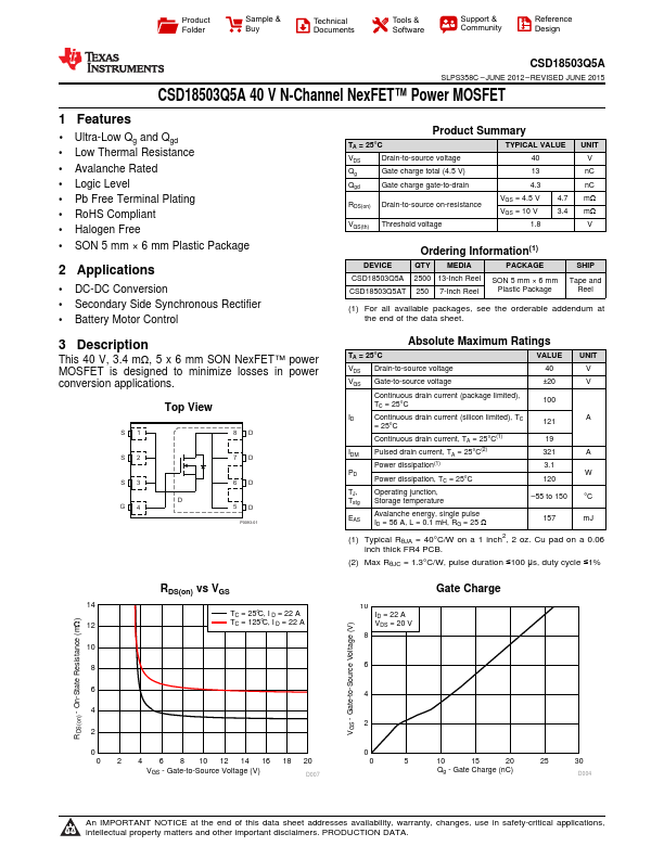
Top View
S1
8D
S2
7D
S3 D
G4
Text added for spacing
6D
5D
P0093-01
Absolute Maximum Ratings
TA = 25°C
VDS Drain-to-source
voltage
VGS Gate-to-source
voltage
Continuous drain current (package limited), TC = 25°C
ID
Continuous drain current (silicon limited), TC
= 25°C
Continuous drain current, TA = 25°C(1)
IDM Pulsed drain cu...