Product Folder
Sample & Buy
Technical Documents
Tools & Software
Support & Community
CSD22202W15
SLPS431B – JUNE 20...
Product Folder
Sample & Buy
Technical Documents
Tools & Software
Support & Community
CSD22202W15
SLPS431B – JUNE 2013 – REVISED DECEMBER 2014
CSD22202W15 P-Channel NexFET™ Power
MOSFET
1 Features
1 Low Resistance Small Footprint 1.5 mm × 1.5 mm Pb Free Gate ESD Protection RoHS Compliant Halogen Free Gate-Source
Voltage Clamp
2 Applications
Battery Management Battery Protection Load Switch Applications
3 Description
The device is designed to deliver the lowest on resistance and gate charge in the smallest outline possible with excellent thermal characteristics in an ultra-low profile. Low on resistance coupled with the small footprint and low profile make the device ideal for battery operated space constrained applications.
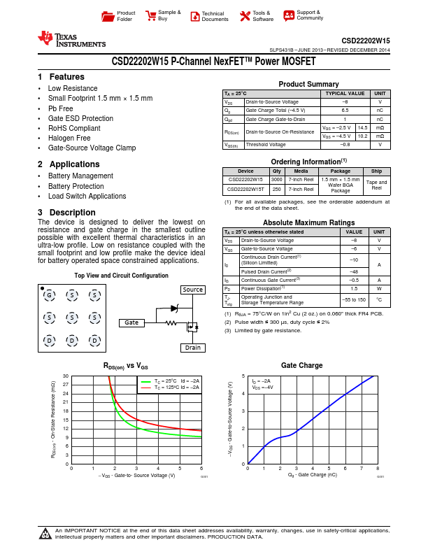
Top View and Circuit Configuration
G
S
S
Source
S
S
S
Gate
DDD
Drain
Product Summary
TA = 25°C
VDS
Drain-to-Source
Voltage
Qg
Gate Charge Total (–4.5 V)
Qgd
Gate Charge Gate-to-Drain
RDS(on) Drain-to-Source On-Resistance
VGS(th) Threshold
Voltage
TYPICAL VALUE
–8
6.5
1
VGS = –2.5 V VGS = –4.5 V
–0.8
14.5 10.2
UNIT V nC nC mΩ mΩ V
Device CSD22202W15 CSD22202W15T
Ordering Information(1)
Qty
Media
Package
3000 7-Inch Reel 250 7-Inch Reel
1.5 mm × 1.5 mm Wafer BGA Package
Ship
Tape and Reel
(1) For all available packages, see the orderable addendum at the end of the data sheet.
Absolute Maximum Ratings
TA = 25°C unless otherwise stated
VDS Drain-to-Source
Voltage
VGS Gate-to-Source
Voltage
Con...