Product Folder
Sample & Buy
Technical Documents
Tools & Software
Support & Community
CSD23382F4
SLPS453C – MAY 2014...
Product Folder
Sample & Buy
Technical Documents
Tools & Software
Support & Community
CSD23382F4
SLPS453C – MAY 2014 – REVISED OCTOBER 2014
CSD23382F4 12 V P-Channel FemtoFET™
MOSFET
1 Features
1 Low On-Resistance Ultra-Low Qg and Qgd Ultra-Small Footprint (0402 Case Size)
– 1.0 mm × 0.6 mm Low Profile
– 0.35 mm Max Height Integrated ESD Protection Diode
– Rated >2 kV HBM – Rated >2 kV CDM Pb Terminal Plating Halogen Free RoHS Compliant
2 Applications
Optimized for Load Switch Applications Optimized for General Purpose Switching
Applications Battery Applications Handheld and Mobile Applications
3 Description
This 66 mΩ, 12 V P-channel FemtoFET™
MOSFET is designed and optimized to minimize the footprint in many handheld and mobile applications. This technology is capable of replacing standard small signal
MOSFETs while providing at least a 60% reduction in footprint size.
.
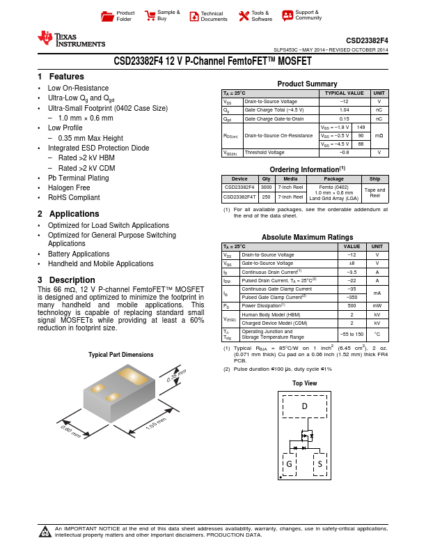
Typical Part Dimensions
0.35 mm
Product Summary
TA = 25°C
VDS
Drain-to-Source
Voltage
Qg
Gate Charge Total (–4.5 V)
Qgd
Gate Charge Gate-to-Drain
RDS(on) Drain-to-Source On-Resistance
VGS(th) Threshold
Voltage
TYPICAL VALUE –12 1.04 0.15
VGS = –1.8 V 149 VGS = –2.5 V 90 VGS = –4.5 V 66
–0.8
UNIT V nC nC
mΩ
V
Device CSD23382F4 CSD23382F4T
Ordering Information(1)
Qty
Media
Package
3000 7-Inch Reel
Femto (0402)
1.0 mm × 0.6 mm 250 7-Inch Reel Land Grid Array (LGA)
Ship
Tape and Reel
(1) For all available packages, see the orderable addendum at the end of the da...