CSD25211W1015
SLPS296A – FEBRUARY 2012 – REVISED JANUARY 2014
CSD25211W1015, P-Channel NexFET™ Power MOSFET
1 Features
...
CSD25211W1015
SLPS296A – FEBRUARY 2012 – REVISED JANUARY 2014
CSD25211W1015, P-Channel NexFET™ Power
MOSFET
1 Features
1 Ultra-Low On Resistance Ultra-Low Qg and Qgd Small Footprint 1.0 mm × 1.5 mm Low Profile 0.62 mm Height Pb Free Gate-Source
Voltage Clamp Gate ESD Protection – 3 kV RoHS Compliant Halogen Free
2 Applications
Battery Management Load Switch Battery Protection
3 Description
The device is designed to deliver the lowest on resistance and gate charge in the smallest outline possible with excellent thermal characteristics in an ultra-low profile.
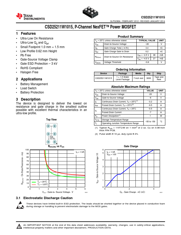
Top View
Product Summary
TA = 25°C unless otherwise stated
VDS
Drain-to-Source
Voltage
Qg
Gate Charge Total (–4.5V)
Qgd
Gate Charge Gate to Drain
RDS(on) Drain-to-Source On Resistance
VGS(th)
Voltage Threshold
TYPICAL VALUE –20 3.4 0.2
VGS = –2.5 V 36 VGS = –4.5 V 27
–0.8
UNIT V nC nC mΩ mΩ V
Device CSD25211W1015
Ordering Information
Package
Media
Qty
1 × 1.5 Wafer Level Package
7-inch reel 3000
Ship
Tape and Reel
Absolute Maximum Ratings
TA = 25°C unless otherwise stated
VDS Drain-to-Source
Voltage
VGS Gate-to-Source
Voltage
ID
Continuous Drain Current, TA = 25°C(1)
IDM Pulsed Drain Current, TA = 25°C(2)
IG
Continuous Drain Current, TA = 25°C Pulsed Drain Current
PD
Power Dissipation(1)
TSTG Storage Temperature Range
TJ
Operating Junction Temperature Range
VALUE -20 -6 -3.2 -9.5 -0.5 -7 1
UNIT V V A A A A W
–55 to 150 °C
(1) Typical RθJA = 119°C/W on 1 inch2 o...