CTH3904NS-T52 N-Channel Enhancement MOSFET
Features
Drain-Source Breakdown Voltage VDSS 40V Drain-Source On-Resista...
CTH3904NS-T52 N-Channel Enhancement
MOSFET
Features
Drain-Source Breakdown
Voltage VDSS 40V Drain-Source On-Resistance
RDS(ON) 9m, at VGS= 10V, ID= 15A RDS(ON) 13m, at VGS= 4.5V, ID= 13A
Continuous Drain Current at TC=25℃ID 39A Advanced high cell density Trench Technology RoHS Compliance & Halogen Free
Description
The CTH3904NS-T52 is the N-Channel logic enhancement mode power field effect transistors are produced using high cell density, DMOS trench technology. This high density process is especially tailored to minimize on-state resistance. These devices are particularly suited for low
voltage application.
Applications
Power Management DC/DC Converter LCD TV & Monitor Display inverter CCFL inverter
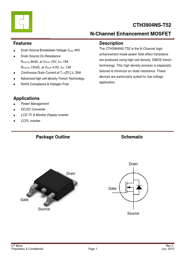
Package Outline
Schematic
Drain
Gate
Source
Drain Gate
Source
CT Micro Proprietary & Confidential
Page 1
Rev 3 Jun, 2015
CTH3904NS-T52 N-Channel Enhancement
MOSFET
Absolute Maximum Rating at 25oC
Symbol
Parameters
VDS Drain-Source
Voltage
VGS Gate-Source
Voltage
ID Continuous Drain Current @TC=25℃
IDM Pulsed Drain Current
PD Total Power Dissipation @TC=25℃
TSTG
Storage Temperature Range
TJ Operating Junction Temperature Range
Thermal Characteristics
Symbol
Parameters
RӨJC
Thermal Resistance Junction-Case
Test Conditions
Test Conditions 40 ±20 39 156 29
-55 to 150 -55 to 150
Min Note Vs V A1 A1 W2 °C °C
Min Typ Max Units Notes -- -- 3.9 oC /W 1,4
CT Micro Proprietary & Confidential
Page 2
Rev 3 Jun, 2015
CTH3904NS-T52 N-Chan...