CTH6106PS-T52 P-Channel Enhancement MOSFET
Features
Drain-Source Breakdown Voltage VDSS -60 V Drain-Source On-Resis...
CTH6106PS-T52 P-Channel Enhancement
MOSFET
Features
Drain-Source Breakdown
Voltage VDSS -60 V Drain-Source On-Resistance
RDS(ON) 14m, at VGS= -10V, IDS= -17A RDS(ON) 16m, at VGS= -4.5V, IDS= -14A
Continuous Drain Current at TC=25℃ ID = -61A Advanced high cell density Trench Technology RoHS Compliance & Halogen Free
Applications
Load Switch Power Management LCD Display inverter DC/DC Converter
Description
The CTH6106PS-T52 uses high performance Trench Technology to provide excellent RDS(ON) and low gate charge which is suitable for most of the synchronous buck converter applications .
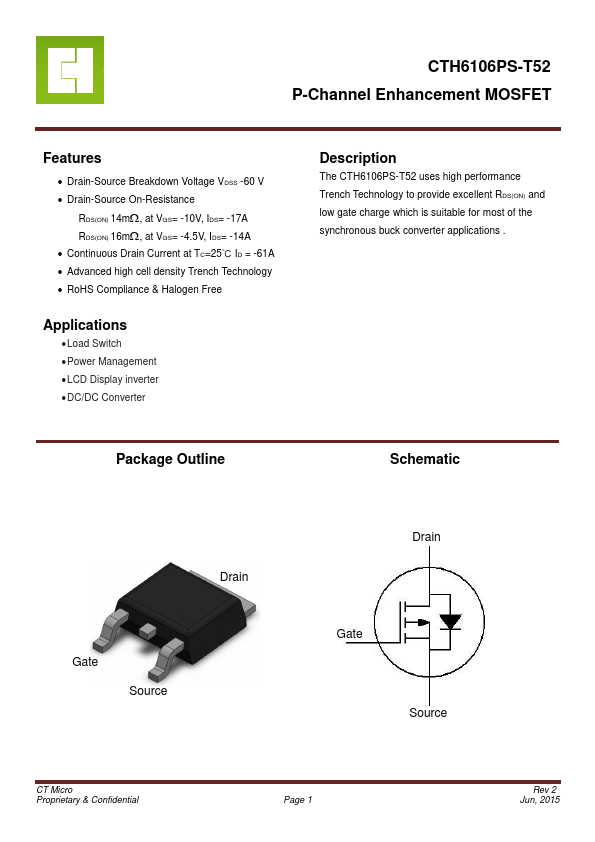
Package Outline
Schematic
Drain
Gate
Source
Drain Gate
Source
CT Micro Proprietary & Confidential
Page 1
Rev 2 Jun, 2015
CTH6106PS-T52 P-Channel Enhancement
MOSFET
Absolute Maximum Rating at 25OC
Symbol
Parameters
VDS Drain-Source
Voltage
VGS Gate-Source
Voltage ID Continuous Drain Current @ TC=25℃
IDM Pulsed Drain Current PD Total Power Dissipation @ TC=25℃
TSTG
Storage Temperature Range
TJ Operating Junction Temperature Range
Thermal Characteristics
Symbol
Parameters
RӨJC
Thermal Resistance Junction-Case
Test Conditions
Ratings -60 ±20 -61 -240 114
-55 to 150 -55 to 150
Units V V A A W 0C 0C
Notes
1 1 2
Min Typ Max Units Notes - - 1.1 C0/W 1,2
CT Micro Proprietary & Confidential
Page 2
Rev 2 Jun, 2015
CTH6106PS-T52 P-Channel Enhancement
MOSFET
Electrical Characteristics TA = 25°C (unless otherwise specified)
Static Characteristics
Symbol...