CTL0196PS-R3 P-Channel Enhancement MOSFET
Features
• Drain-Source Breakdown Voltage VDSS -60 V • Drain-Source On-Resist...
CTL0196PS-R3 P-Channel Enhancement
MOSFET
Features
Drain-Source Breakdown
Voltage VDSS -60 V Drain-Source On-Resistance
RDS(ON) 170mΩ, at VGS= -10V, ID= -1.8A RDS(ON) 200mΩ, at VGS= -4.5V, ID= -1.4A
℃ Continuous Drain Current at TC=25 ID = -1.9A
Advanced high cell density Trench Technology RoHS Compliance & Halogen Free
Description
The CTL0196PS-R3 is the P-Channel logic enhancement mode power field effect transistors are produced using high cell density, DMOS trench technology. This high density process is especially tailored to minimize on-state resistance.
Applications
Power Management Battery Powered System DC/DC Converter Load Switch DSC LCD Display inverter
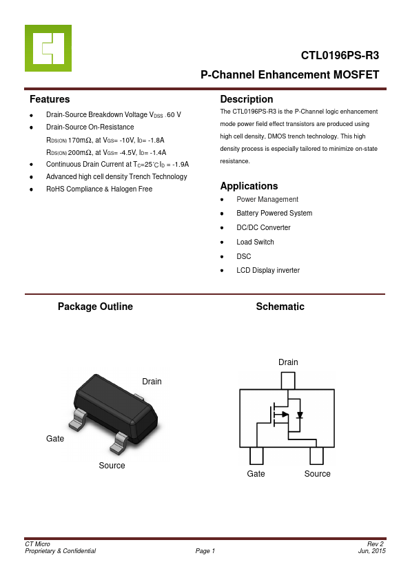
Package Outline
Schematic
Drain
Drain
Gate
Source
Gate
Source
CT Micro Proprietary & Confidential
Page 1
Rev 2 Jun, 2015
CTL0196PS-R3 P-Channel Enhancement
MOSFET
Absolute Maximum Rating at 25oC
Symbol
Parameters
VDS Drain-Source
Voltage
VGS Gate-Source
Voltage
ID Continuous Drain Current
IDM Pulsed Drain Current
PD Total Power Dissipation
TSTG
Storage Temperature Range
TJ Operating Junction Temperature Range
Thermal Characteristics
Symbol
Parameters
RӨJA4
Thermal Resistance Junction-Ambient (t=10s)
Test Conditions
Test Conditions -60 ±20 -1.9 -7.6 1.4
-55 to 150 -55 to 150
Min Notes V V A1 A1 W2 °C °C
Min Typ Max Units Notes -- 90 -- oC /W 1,4
CT Micro Proprietary & Confidential
Page 2
Rev 2 Jun, 2015
CTL0196PS-R3 P-Channel Enhancement
MOSFET
Electrical Cha...