CTL0404NS-R3 N-Channel Enhancement MOSFET
Features
• Drain-Source Breakdown Voltage VDSS 40 V • Drain-Source On-Resista...
CTL0404NS-R3 N-Channel Enhancement
MOSFET
Features
Drain-Source Breakdown
Voltage VDSS 40 V Drain-Source On-Resistance
RDS(ON) 32mΩ, at VGS= 10V, ID= 4.0A RDS(ON) 50mΩ, at VGS= 4.5V, ID= 3.0A
℃ Continuous Drain Current at TA=25 ID =4.0A
Advanced high cell density Trench Technology RoHS Compliance & Halogen Free
Description
The CTL0404NS-R3 is the N-Channel logic enhancement mode power field effect transistors are produced using high cell density, DMOS trench technology. This high density process is especially tailored to minimize on-state resistance.
Applications
Power Management Portable Equipment DC/DC Converter Load Switch
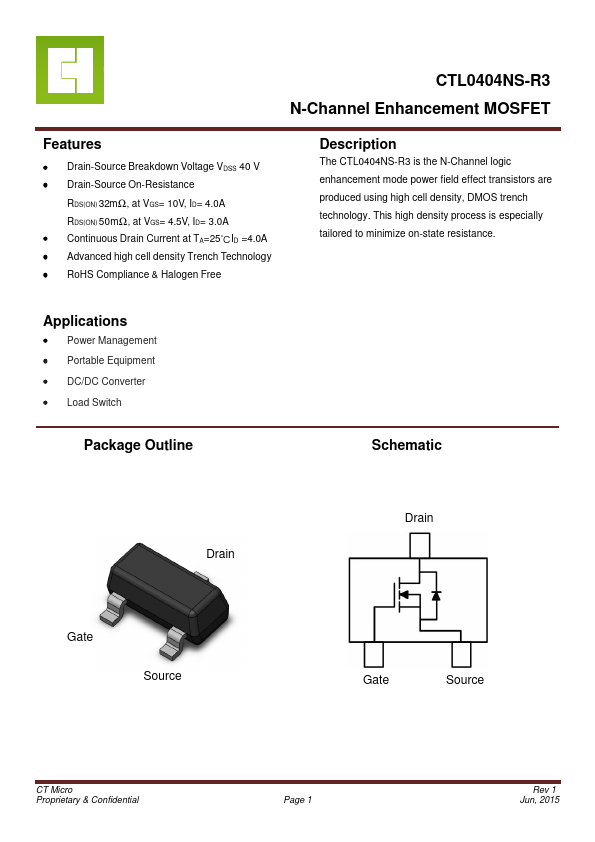
Package Outline
Schematic
Drain
Drain
Gate
Source
Gate
Source
CT Micro Proprietary & Confidential
Page 1
Rev 1 Jun, 2015
CTL0404NS-R3 N-Channel Enhancement
MOSFET
Absolute Maximum Rating at 25oC
Symbol
Parameters
VDS Drain-Source
Voltage
VGS Gate-Source
Voltage
℃ID Continuous Drain Current @TA=25
IDM Pulsed Drain Current
℃PD Total Power Dissipation @TA=25
TSTG
Storage Temperature Range
TJ Operating Junction Temperature Range
Thermal Characteristics
Symbol
Parameters
RӨJA4
Thermal Resistance Junction-Ambient (t=10s)
Test Conditions
Test Conditions 40 ±20 4 16 1.4
-55 to 150 -55 to 150
Min Notes V V A1 A1 W2 °C °C
Min Typ Max Units Notes -- 120 -- oC /W 1,4
CT Micro Proprietary & Confidential
Page 2
Rev 1 Jun, 2015
CTL0404NS-R3 N-Channel Enhancement
MOSFET
Electrical Characteristics TA = 25°C (unless ot...