CTLM13PS05-R3 P-Channel Enhancement MOSFET
Features
• Drain-Source Breakdown Voltage VDSS - 50 V • Drain-Source On-Resi...
CTLM13PS05-R3 P-Channel Enhancement
MOSFET
Features
Drain-Source Breakdown
Voltage VDSS - 50 V Drain-Source On-Resistance
RDS(ON) 5Ω, at VGS= - 5.0V, IDS= - 100mA
℃ Continuous Drain Current at TA=25 ID = -130mA
Advanced high cell density Trench Technology RoHS Compliance & Halogen Free
Applications
Power Management Portable Equipment Battery Powered System DC/DC Converter Load Switch
Description
The CTLM13PS05-R3 uses high performance Trench Technology to provide excellent RDS(ON) and low gate charge which is suitable for most of the synchronous buck converter applications .
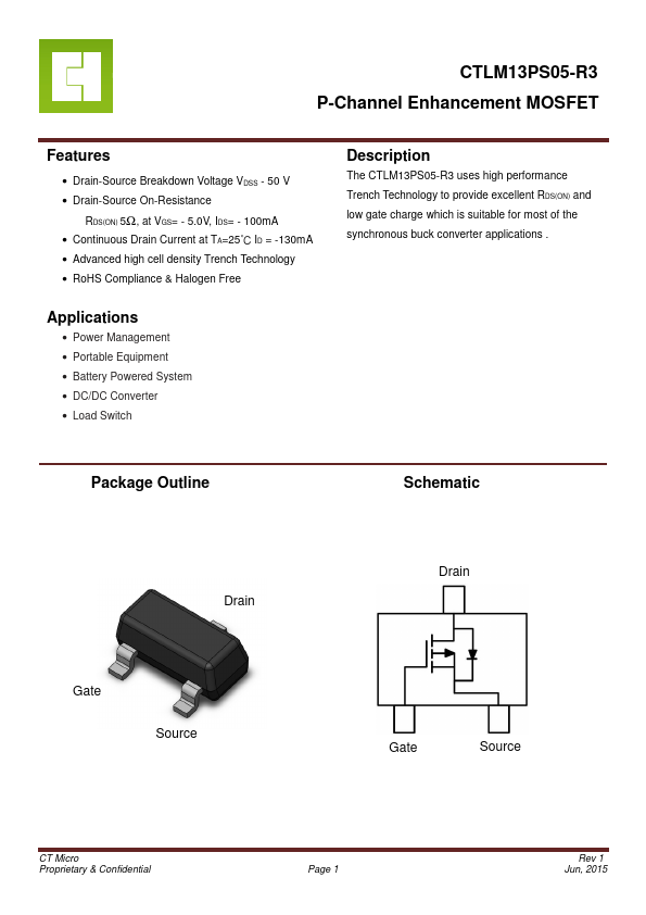
Package Outline
Schematic
Drain
Drain
Gate
Source
Gate
Source
CT Micro Proprietary & Confidential
Page 1
Rev 1 Jun, 2015
CTLM13PS05-R3 P-Channel Enhancement
MOSFET
Absolute Maximum Rating at 25oC
Symbol
Parameters
VDS Drain-Source
Voltage
VGS Gate-Source
Voltage
℃ID Continuous Drain Current @TA=25
IDM Pulsed Drain Current
℃PD Total Power Dissipation @TA=25
TSTG
Storage Temperature Range
TJ Operating Junction Temperature Range
Thermal Characteristics
Symbol
Parameters
RӨJA
Thermal Resistance Junction-Ambient (t=10s)
Test Conditions
Ratings -50 ±20 -0.13 -0.52 0.225
-55 to 150 -55 to 150
Units V V A A W oC oC
Notes
1 1 2
Min Typ Max Units Notes
-
555
-
oC /W
1,4
CT Micro Proprietary & Confidential
Page 2
Rev 1 Jun, 2015
CTLM13PS05-R3 P-Channel Enhancement
MOSFET
Electrical Characteristics TA = 25°C (unless otherwise specified)
Static Characteris...