Clock Generator
CY24271
Rambus® XDR™ Clock Generator
Rambus® XDR™ Clock Generator
Features
■ Meets Rambus Extended Data Rate (XDR™) cl...
Description
CY24271
Rambus® XDR™ Clock Generator
Rambus® XDR™ Clock Generator
Features
■ Meets Rambus Extended Data Rate (XDR™) clocking requirements
■ 25 ps typical cycle-to-cycle jitter ❐ 135 dBc/Hz typical phase noise at 20 MHz offset
■ 100 or 133 MHz differential clock input ■ 300–800 MHz high speed clock support
■ Quad (open drain) differential output drivers ■ Supports frequency multipliers: 3, 4, 5, 6, 8, 9/2, 15/2, and 15/4 ■ Spread Aware™ ■ 2.5 V operation ■ 28-pin TSSOP package
Functional Description
For a complete list of related documentation, click here.
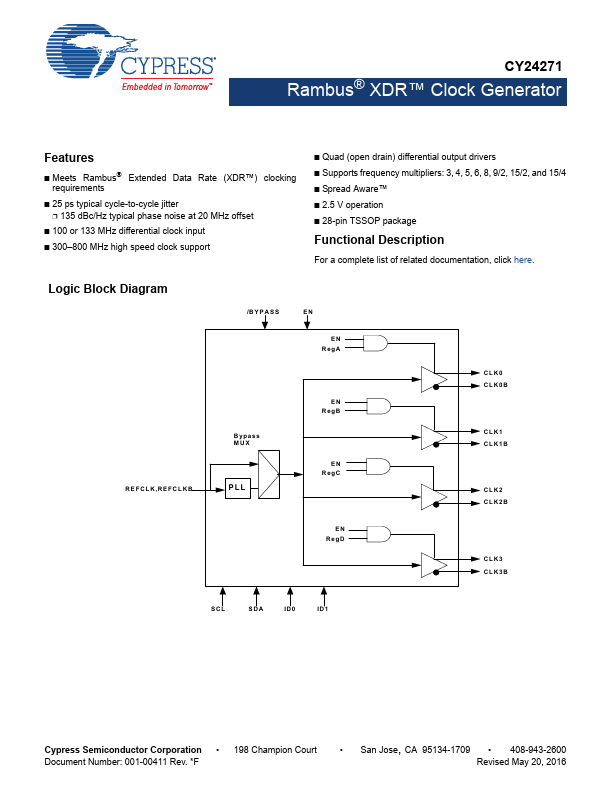
Logic Block Diagram
/B YPA SS
EN
Bypass MUX
REFCLK,REFC LKB
PLL
EN RegA
EN RegB
EN RegC
CLK0 CLK0B
CLK1 CLK1B
CLK2 CLK2B
EN RegD
CLK3 CLK3B
SCL
SDA ID0 ID1
Cypress Semiconductor Corporation 198 Champion Court Document Number: 001-00411 Rev. *F
San Jose, CA 95134-1709 408-943-2600
Revised May 20, 2016
CY24271
Contents
Pinouts .................................................
Similar Datasheet