www.DataSheet4U.com
CY2SSTV16859
13-Bit to 26-Bit Registered Buffer PC2700-/PC3200-Compliant
Features
• Differential c...
www.DataSheet4U.com
CY2SSTV16859
13-Bit to 26-Bit Registered Buffer PC2700-/PC3200-Compliant
Features
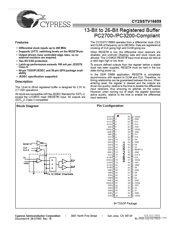
Differential clock inputs up to 280 MHz Supports LVTTL switching levels on the RESET# pin Output drivers have controlled edge rates, so no external resistors are required. Two KV ESD protection Latch-up performance exceeds 100 mA per JESD78, Class II 64-pin TSSOP/JEDEC and 56-pin QFN package availability JEDEC specification supported The CY2SSTV16859 operates from a differential clock (CLK and CLK#) of frequency up to 280 MHz. Data are registered at crossing of CLK going high and CLK# going low. When RESET# is low, the differential input receivers are disabled, and undriven (floating) data and clock inputs are allowed. The LV
CMOS RESET# input must always be held at a valid logic high or low level. To ensure defined outputs from the register before a stable clock has been supplied, RESET# must be held in the low state during power up. In the DDR DIMM application, RESET# is completely asynchronous with respect to CLK# and CLK. Therefore, no timing relationship can be guaranteed between the two. When entering reset, the register is cleared and the outputs are driven low quickly, relative to the time to disable the differential input receivers, thus ensuring no glitches on the output. However, when coming out of reset, the register becomes active quickly, relative to the time to enable the differential input receivers.
Description
This 13-bit to 26-bit registered...