QUAD 2-INPUT MULTIPLEXER
D Function, Pinout, and Drive Compatible
With FCT and F Logic
D Reduced VOH (Typically = 3.3 V) Version of
Equivalent FC...
Description
D Function, Pinout, and Drive Compatible
With FCT and F Logic
D Reduced VOH (Typically = 3.3 V) Version of
Equivalent FCT Functions
D Edge-Rate Control Circuitry for
Significantly Improved Noise Characteristics
D Ioff Supports Partial-Power-Down Mode
Operation
D Matched Rise and Fall Times D Fully Compatible With TTL Input and
Output Logic Levels
D ESD Protection Exceeds JESD 22
− 2000-V Human-Body Model (A114-A) − 200-V Machine Model (A115-A) − 1000-V Charged-Device Model (C101)
D 64-mA Output Sink Current
32-mA Output Source Current
D 3-State Outputs
CY74FCT257T
QUAD 2-INPUT MULTIPLEXER
WITH 3-STATE OUTPUTS
SCCS019D − MAY 1994 − REVISED NOVEMBER 2001
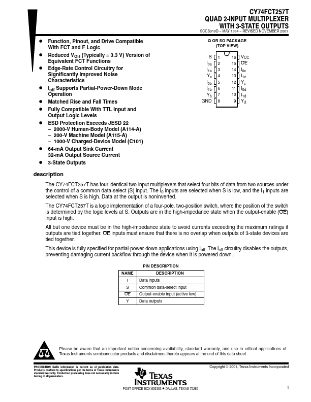
Q OR SO PACKAGE (TOP VIEW)
S
I0a I1a Ya I0b I1b Yb GND
1 2 3 4 5 6 7 8
16 VCC 15 OE
14 I0c 13 I1c 12 Yc 11 I0d 10 I1d 9 Yd
description
The CY74FCT257T has four identical two-input multiplexers that select four bits of data from two sources under the control of a common data-select (S) input. The I0 inputs are selected when S is low, and the I1 inputs are selected when S is high. Data at the output is noninverted.
The CY74FCT257T is a logic implementation of a four-pole, two-position switch, where the position of the switch is determined by the logic levels at S. Outputs are in the high-impedance state when the output-enable (OE) input is high.
All but one device must be in the high-impedance state to avoid currents exceeding the maximum ratings if outputs are tied together. OE inputs must ensure that there is no overlap w...
Similar Datasheet