8-BIT REGISTERED TRANSCEIVER
D Function and Pinout Compatible With FCT
and F Logic
D 25-Ω Output Series Resistors Reduce
Transmission-Line Reflection...
Description
D Function and Pinout Compatible With FCT
and F Logic
D 25-Ω Output Series Resistors Reduce
Transmission-Line Reflection Noise
D Reduced VOH (Typically = 3.3 V) Versions
of Equivalent FCT Functions
D Edge-Rate Control Circuitry for
Significantly Improved Noise
Characteristics
D Ioff Supports Partial-Power-Down Mode
Operation
D Matched Rise and Fall Times D Fully Compatible With TTL Input and
Output Logic Levels
D ESD Protection Exceeds JESD 22
– 2000-V Human-Body Model (A114-A)
– 200-V Machine Model (A115-A)
– 1000-V Charged-Device Model (C101)
D 12-mA Output Sink Current
15-mA Output Source Current
D Independent Register for A and B Buses D Multiplexed Real-Time and Stored Data
Transfer
D 3-State Outputs
CY74FCT2652T 8-BIT REGISTERED TRANSCEIVER
WITH 3-STATE OUTPUTS
SCCS044B – MAY 1994 – REVISED NOVEMBER 2001
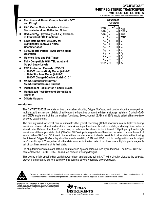
Q PACKAGE (TOP VIEW)
CPAB
SAB
GAB
A1 A2 A3 A4 A5 A6 A7 A8 GND
1 2 3 4 5 6 7 8 9 10 11 12
24 VCC 23 CPBA
22 SBA
21 GBA
20 B1 19 B2 18 B3 17 B4 16 B5 15 B6 14 B7 13 B8
description
The CY74FCT2652T consists of bus transceiver circuits, D-type flip-flops, and control circuitry arranged for multiplexed transmission of data directly from the input bus or from the internal storage registers. Control (GAB and GBA) inputs control the transceiver functions. Select-control (SAB and SBA) inputs select either real-time or stored data transfer.
The circuitry used for select control eliminates the typical decoding glitch that occurs in a multiplexer during transition between sto...
Similar Datasheet