36-Mbit (1 M x 36/2 M x 18) Pipelined SRAM
CY7C1460BV25 CY7C1462BV25
36-Mbit (1 M × 36/2 M × 18) Pipelined SRAM with NoBL™ Architecture
36-Mbit (1 M × 36/2 M × 18...
Description
CY7C1460BV25 CY7C1462BV25
36-Mbit (1 M × 36/2 M × 18) Pipelined SRAM with NoBL™ Architecture
36-Mbit (1 M × 36/2 M × 18) Pipelined SRAM with NoBL™ Architecture
Features
■ Pin-compatible and functionally equivalent to ZBT™ ■ Supports 250-MHz bus operations with zero wait states
❐ Available speed grades is 250 MHz ■ Internally self-timed output buffer control to eliminate the need
to use asynchronous OE ■ Fully registered (inputs and outputs) for pipelined operation ■ Byte Write capability ■ 2.5 V core power supply ■ 2.5 V I/O power supply ■ Fast clock-to-output times
❐ 2.6 ns (for 250-MHz device) ■ Clock enable (CEN) pin to suspend operation ■ Synchronous self-timed writes ■ CY7C1460BV25, CY7C1462BV25 available in Pb-free
165-ball FBGA package and CY7C1462BV25 available in JEDEC-standard Pb-free 100-pin TQFP package ■ IEEE 1149.1 JTAG-Compatible Boundary Scan ■ Burst capability – linear or interleaved burst order ■ “ZZ” sleep mode option ...
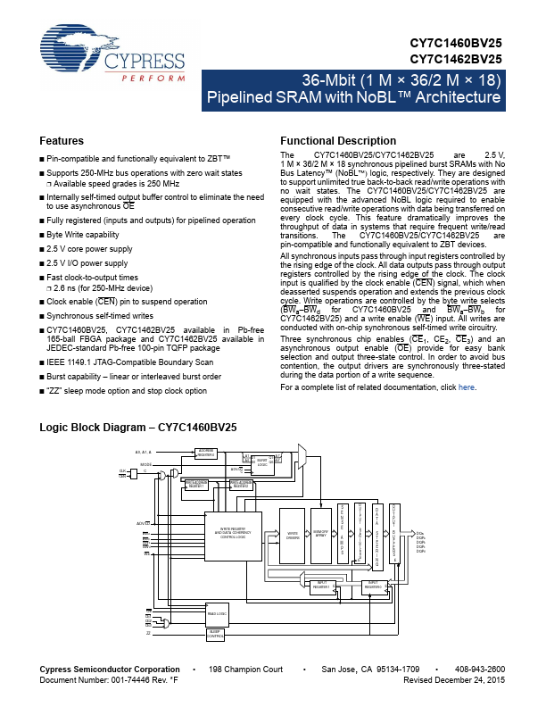
Similar Datasheet