CY7C4281 CY7C4291
64K/128K x 9 Deep Sync FIFOs
Features
• High-speed, low-power, first-in first-out (FIFO) memories • 6...
CY7C4281 CY7C4291
64K/128K x 9 Deep Sync FIFOs
Features
High-speed, low-power, first-in first-out (FIFO) memories 64K × 9 (CY7C4281) 128K × 9 (CY7C4291) 0.5-micron
CMOS for optimum speed/power High-speed 100-MHz operation (10-ns read/write cycle times) Low power — ICC= 40 mA — ISB = 2 mA Fully asynchronous and simultaneous read and write operation Empty, Full, and programmable Almost Empty and Almost Full status flags TTL compatible Output Enable (OE) pin Independent read and write enable pins Center power and ground pins for reduced noise Supports free-running 50% duty cycle clock inputs Width Expansion Capability 32-pin PLCC Pin-compatible density upgrade to CY7C42X1 family Pin-compatible density upgrade to IDT72201/11/21/31/41/51
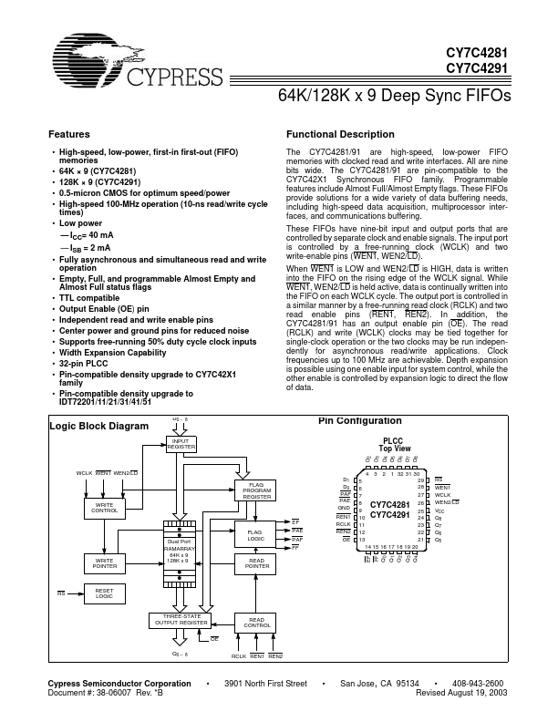
D0 − 8
Functional Description
The CY7C4281/91 are high-speed, low-power FIFO memories with clocked read and write interfaces. All are nine bits wide. The CY7C4281/91 are pin-compatible to the CY7C42X1 Synchronous FIFO family. Programmable features include Almost Full/Almost Empty flags. These FIFOs provide solutions for a wide variety of data buffering needs, including high-speed data acquisition, multiprocessor interfaces, and communications buffering. These FIFOs have nine-bit input and output ports that are controlled by separate clock and enable signals. The input port is controlled by a free-running clock (WCLK) and two write-enable pins (WEN1, WEN2/LD). When WEN1 is LOW and WEN2/LD is HIGH, data is written...