2SD1367
Silicon NPN Epitaxial
Application
• Low frequency power amplifier • Complementary pair with 2SB1001
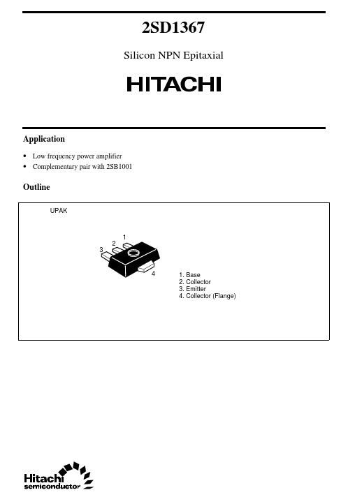
Outline
UP...
2SD1367
Silicon NPN Epitaxial
Application
Low frequency power amplifier Complementary pair with 2SB1001
Outline
UPAK
1 3 2
4
1. Base 2. Collector 3. Emitter 4. Collector (Flange)
2SD1367
Absolute Maximum Ratings (Ta = 25°C)
Item Collector to base
voltage Collector to emitter
voltage Emitter to base
voltage Collector current Collector peak current Collector power dissipation Junction temperature Storage temperature Symbol VCBO VCEO VEBO IC iC(peak)* PC * Tj Tstg
2 1
Ratings 20 16 6 2 3 1 150 –55 to +150
Unit V V V A A W °C °C
Notes: 1. PW ≤ 10 ms, Duty cycle ≤ 20%. 2. Value on the alumina ceramic board (12.5 × 20 × 0.7 mm)
Electrical Characteristics (Ta = 25°C)
Item Collector to base breakdown
voltage Symbol V(BR)CBO Min 20 16 6 — —
1
Typ — — — —
Max — — — 0.1 0.1
Unit V V V µA µA
Test conditions I C = 10 µA, IE = 0 I C = 1 mA, RBE = ∞ I E = 10 µA, IC = 0 VCB = 16 V, IE = 0 VEB = 5 V, IC = 0 VCE = 2 V, IC = 0.1 A, Pulse
Collector to emitter breakdown V(BR)CEO
voltage Emitter to base breakdown
voltage Collector cutoff current Emitter cutoff current DC current transfer ratio Collector to emitter saturation
voltage Base to emitter saturation
voltage Gain bandwidth product Collector output capacitance Note: Mark hFE BA 100 to 200 BB 160 to 320 V(BR)EBO I CBO I EBO hFE*
100 — — — — BC
— 0.15 0.9 100 20
500 0.3 1.2 — — V V MHz pF
VCE(sat) VBE(sat) fT Cob
I C = 1 A, IB = 0.1 A, Pulse I C = 1 A, IB = 0.1 A, Pulse VCE = 2 V, IC = 10 mA VCB = 10 V, IE = 0, f = 1 ...