Tentative DA26101
Silicon epitaxial planar type
For high speed switching circuits Marking Symbol : A1 Package Code : ML2...
Tentative DA26101
Silicon epitaxial planar type
For high speed switching circuits Marking Symbol : A1 Package Code : ML2-N3-B Absolute Maximum Ratings Ta = 25 °C
Parameter
Reverse
voltage Maximum peak reverse
voltage Forward current Peak forward current Non-repetitive peak forward surge current *1 Junction temperature Storage temperature Note: 1. *1 t = 1 s
DA26101
Total pages page
Symbol
VR VRM IF IFM IFSM Tj Tstg
Rating
80 80 100 225 500 125 -55 to +125
Unit
V V mA mA mA °C °C
Pin name
1. Cathode 2. Anode
Electrical Characteristics Ta = 25 °C±3 °C
Parameter
Forward
voltage Reverse
voltage Reverse current Terminal capacitance Reverse recovery time
*1
Symbol
VF VR IR Ct trr
Conditions
IF = 100 mA IR = 100 μA VR = 80 V VR = 0 V , f = 1 MHz IF = 10 mA, VR = 6 V Irr = 0.25 x IR
Min
80
Typ
0.92
Max
1.20 100 1.2 3
Unit
V V nA pF ns
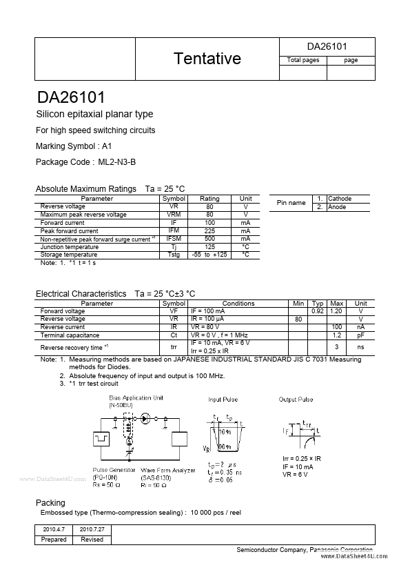
Note: 1. Measuring methods are based on JAPANESE INDUSTRIAL STANDARD JIS C 7031 Measuring methods for Diodes. 2. Absolute frequency of input and output is 100 MHz. 3. *1 trr test circuit
www.DataSheet4U.com
Irr = 0.25 × IR IF = 10 mA VR = 6 V
Packing
Embossed type (Thermo-compression sealing) : 10 000 pcs / reel
2010.4.7 2010.7.27
Prepared
Revised Semiconductor Company, Panasonic Corporation
ML2-N3-B
Unit: mm
0.60 ±0.05 2
0.39 −0.03
+0.01
1 0.05 ±0.03 0.25 ±0.05 0.50 ±0.05 0.25 ±0.05
1.00 ±0.05
0.65 ±0.01
www.DataSheet4U.com
0.05 ±0.03
Request for your special attention and precautions in using the technical information and...