matched dual n-channel JFETs
H
Siliconix
designed for • • •
Performance Curves NCB-D See Sedion 4
• Wideband Differe...
matched dual n-channel JFETs
H
Siliconix
designed for
Performance Curves NCB-D See Sedion 4
Wideband Differential
Amplifiers
Commutators
ABSOLUTE MAXIMUM RATINGS (25°C)
Gate-Gate
Voltage .......................... ±80V
Gate-Drain or Gate-Source
Voltage .......... -40 V Gate Current .................... 50 rnA Device Dissipation (Each Side), TA = 25°C
(Derate 2.2 mW/oC) .............. 325mW
Total Device Dissipation, TA = 25°C (Derate 3.3 mW/oC) ......... 650mW
Storage Temperature Range ....... -65 to +200°C
Lead Temperature (1/16" from case for 10 seconds) ..............300°C
BENEFITS
High Gain 7500 tLmho Minimum gfs
Specified Matching Characteristics
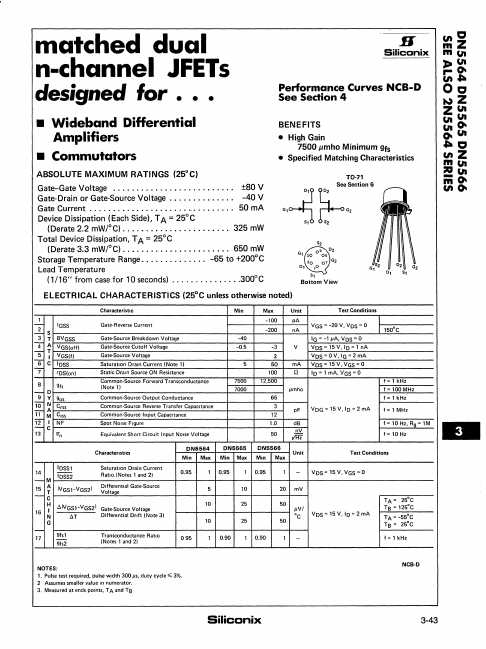
TO-71 See Section 6
~~G, Gz S, 82
S2
G,
30
0' 02 06
20 0 7 G2 0, ,0
s,
Bottom View
.4. "
ELECTRICAL CHARACTERISTICS (25°C unless otherwise noted)
1
1'2
I~
14
5'
S T A T 1
IGSS
BVGSS VGS(off) VGS(I)
6" C lOSS
1" rOS(on)
8 91.
g-
10 'iT
O
V
N A M
90.
Crss
C1SS
-i2
13
1 C
NF ifn
Characteristic
Gate-Reverse Current
Gate-Source Breakdown
Voltage Gate-Source Cutoff
Voltage Gate-Source
Voltage Saturation Drain Current (Note 1) Static Drain Source ON Resistance Common-Source Forward Transconductance
(Nol.')
Common-Source Output Conductance Common-Source Reverse Transfer Capacitance Common·Source Input Capacitance Spot NOise Figure
Equivalent Short Circuit Input NOise
Voltage
Characteristics
14 -M
IOSS1 IOSS2
Saturation Drain Current
RaIla, (Nol.'...