DS14C89A DS14C89AT Quad CMOS Receiver
February 1996
DS14C89A DS14C89AT Quad CMOS Receiver
General Description
The DS14...
DS14C89A DS14C89AT Quad
CMOS Receiver
February 1996
DS14C89A DS14C89AT Quad
CMOS Receiver
General Description
The DS14C89A DS14C89AT pin-for-pin compatible to the DS1489A MC1489A are receivers designed to interface data terminal equipment (DTE) with data circuit-terminating equipment (DCE) These devices translate levels conforming to EIA-232E and CCITT V 28 standards to TTL
CMOS logic levels The device is fabricated in low threshold
CMOS metal gate technology The device provides very low power consumption compared to their bipolar equivalents 900 mA (DS14C89A) versus 26 mA (DS1489A) The DS14C89A DS14C89AT provide on chip noise filtering which eliminates the need for external response control filter
capacitors When replacing the DS1489A with the DS14C89A DS14C89AT the response control filter pins can be tied high low or not connected
Features
Y Y
Y Y Y
Meets EIA TIA-232-E and CCITT V 28 Standards Industrial Temperature Range b 40 C to a 85 C – DS14C89AT LOW Power consumption On chip noise filter Available in SOIC Package
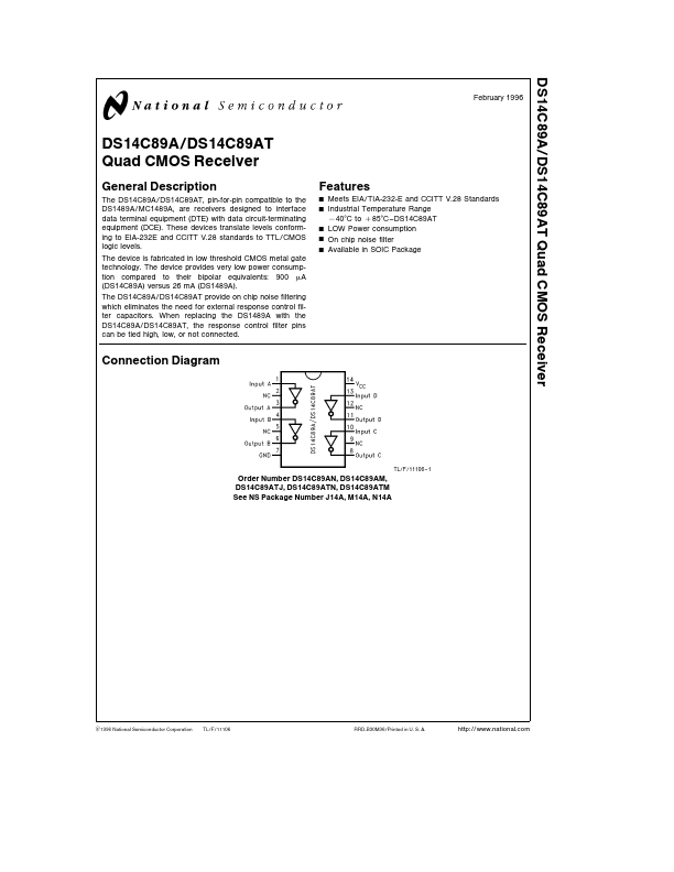
Connection Diagram
TL F 11106 – 1
Order Number DS14C89AN DS14C89AM DS14C89ATJ DS14C89ATN DS14C89ATM See NS Package Number J14A M14A N14A
C1996 National Semiconductor Corporation
TL F 11106
RRD-B30M36 Printed in U S A
http
www national com
Absolute Maximum Ratings (Note 1)
If Military Aerospace specified devices are required please contact the National Semiconductor Sales Office Distributors for availability and specifications VCC
a 6V b 30V to a ...