DS90C032 LVDS Quad CMOS Differential Line Receiver
June 1998
DS90C032 LVDS Quad CMOS Differential Line Receiver
Genera...
DS90C032 LVDS Quad
CMOS Differential Line Receiver
June 1998
DS90C032 LVDS Quad
CMOS Differential Line Receiver
General Description
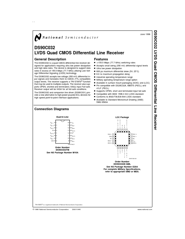
The DS90C032 is a quad
CMOS differential line receiver designed for applications requiring ultra low power dissipation and high data rates. The device is designed to support data rates in excess of 155.5 Mbps (77.7 MHz) utilizing Low
Voltage Differential Signaling (LVDS) technology. The DS90C032 accepts low
voltage (350 mV) differential input signals and translates them to
CMOS (TTL compatible) output levels. The receiver supports a TRI-STATE ® function that may be used to multiplex outputs. The receiver also supports OPEN, shorted and terminated (100Ω) input Fail-safe. Receiver output will be HIGH for all fail-safe conditions. The DS90C032 and companion line driver (DS90C031) provide a new alternative to high power psuedo-ECL devices for high speed point-to-point interface applications.
Features
n n n n n n n n n n n n n
> 155.5 Mbps (77.7 MHz) switching rates Accepts small swing (350 mV) differential signal levels Ultra low power dissipation 600 ps maximum differential skew (5V, 25˚C) 6.0 ns maximum propagation delay Industrial operating temperature range Military operating temperature range option Available in surface mount packaging (SOIC) and (LCC) Pin compatible with DS26C32A, MB570 (PECL) and 41LF (PECL) Supports OPEN, short and terminated input fail-safe Compatible with IEEE 1596.3 SCI LVDS standard Conforms to ANSI/TIA/EIA-644 LVDS s...