DS90C032BLVDS Quad CMOS Differential Line Receiver
September 2003
DS90C032B
LVDS Quad CMOS Differential Line Receiver...
DS90C032BLVDS Quad
CMOS Differential Line Receiver
September 2003
DS90C032B
LVDS Quad
CMOS Differential Line Receiver
General Description
TheDS90C032B is a quad
CMOS differential line receiver designed for applications requiring ultra low power dissipation and high data rates. The device is designed to support data rates in excess of 155.5 Mbps (77.7 MHz) utilizing Low
Voltage Differential Signaling (LVDS) technology.
TheDS90C032B accepts low
voltage (350 mV) differential input signals and translates them to
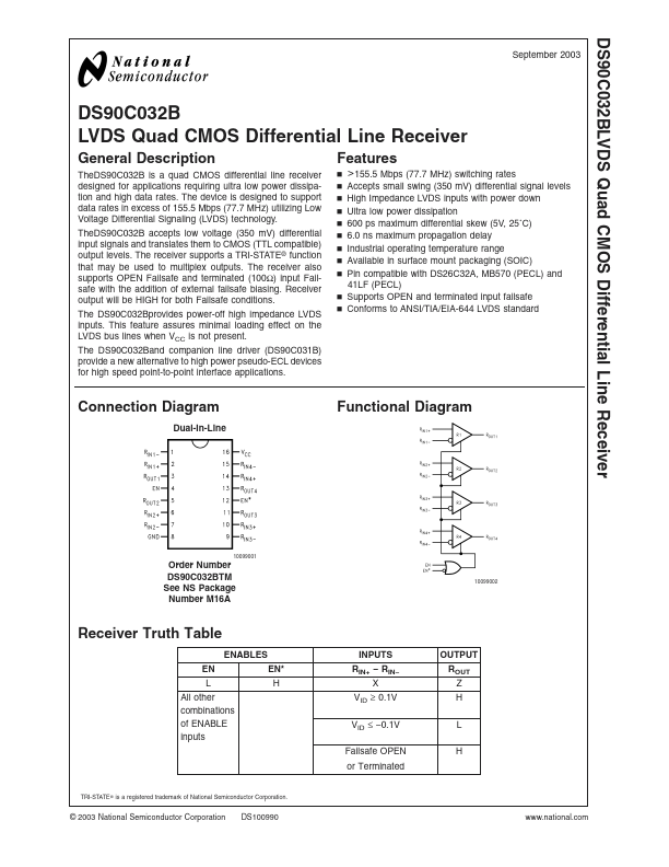
CMOS (TTL compatible) output levels. The receiver supports a TRI-STATE® function that may be used to multiplex outputs. The receiver also supports OPEN Failsafe and terminated (100Ω) input Failsafe with the addition of external failsafe biasing. Receiver output will be HIGH for both Failsafe conditions.
The DS90C032Bprovides power-off high impedance LVDS inputs. This feature assures minimal loading effect on the LVDS bus lines when VCC is not present.
The DS90C032Band companion line driver (DS90C031B) provide a new alternative to high power pseudo-ECL devices for high speed point-to-point interface applications.
Features
n >155.5 Mbps (77.7 MHz) switching rates
n Accepts small swing (350 mV) differential signal levels n High Impedance LVDS inputs with power down n Ultra low power dissipation n 600 ps maximum differential skew (5V, 25˚C) n 6.0 ns maximum propagation delay n Industrial operating temperature range n Available in surface mount packaging (SOIC) n Pin comp...