DS90C401 Dual Low Voltage Differential Signaling (LVDS) Driver
June 1998
DS90C401 Dual Low Voltage Differential Signal...
DS90C401 Dual Low
Voltage Differential Signaling (LVDS) Driver
June 1998
DS90C401 Dual Low
Voltage Differential Signaling (LVDS) Driver
General Description
The DS90C401 is a dual driver device optimized for high data rate and low power applications. This device along with the DS90C402 provides a pair chip solution for a dual high speed point-to-point interface. The DS90C401 is a current mode driver allowing power dissipation to remain low even at high frequency. In addition, the short circuit fault current is also minimized. The device is in a 8 lead small outline package. The differential driver outputs provides low EMI with its low output swings typically 340 mV.
Features
n n n n n Ultra low power dissipation Operates above 155.5 Mbps Standard TIA/EIA-644 8 Lead SOIC Package saves space Low Differential Output Swing typical 340 mV
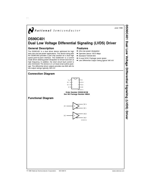
Connection Diagram
DS100013-1
Order Number DS90C401M See NS Package Number M08A
Functional Diagram
DS100013-2
© 1998 National Semiconductor Corporation
DS100013
www.national.com
Absolute Maximum Ratings (Note 1)
If Military/Aerospace specified devices are required, please contact the National Semiconductor Sales Office/ Distributors for availability and specifications. Supply
Voltage (VCC) −0.3V to +6V −0.3V to (VCC + 0.3V) Input
Voltage (DIN) −0.3V to (VCC + 0.3V) Output
Voltage (DOUT+, DOUT−) Short Circuit Duration Continuous (DOUT+, DOUT−) Maximum Package Power Dissipation @ +25˚C M Package 1068 mW Derate M Package 8.5 mW/˚C above +...