DS90CR287, DS90CR288A
www.ti.com
SNLS056G – OCTOBER 1999 – REVISED MARCH 2013
DS90CR287/DS90CR288A +3.3V Rising Edge ...
DS90CR287, DS90CR288A
www.ti.com
SNLS056G – OCTOBER 1999 – REVISED MARCH 2013
DS90CR287/DS90CR288A +3.3V Rising Edge Data Strobe LVDS 28-Bit Channel Link - 85MHz
Check for Samples: DS90CR287, DS90CR288A
FEATURES
1
20 to 85 MHz Shift Clock Support 50% Duty Cycle on Receiver Output Clock 2.5 / 0 ns Set & Hold Times on TxINPUTs Low Power Consumption ±1V Common-Mode Range (around +1.2V) Narrow Bus Reduces Cable Size and Cost Up to 2.38 Gbps Throughput Up to 297.5 Mbytes/sec Bandwidth 345 mV (typ) Swing LVDS Devices for Low EMI PLL Requires no External Components Rising Edge Data Strobe Compatible with TIA/EIA-644 LVDS Standard Low Profile 56-Lead TSSOP Package
DESCRIPTION
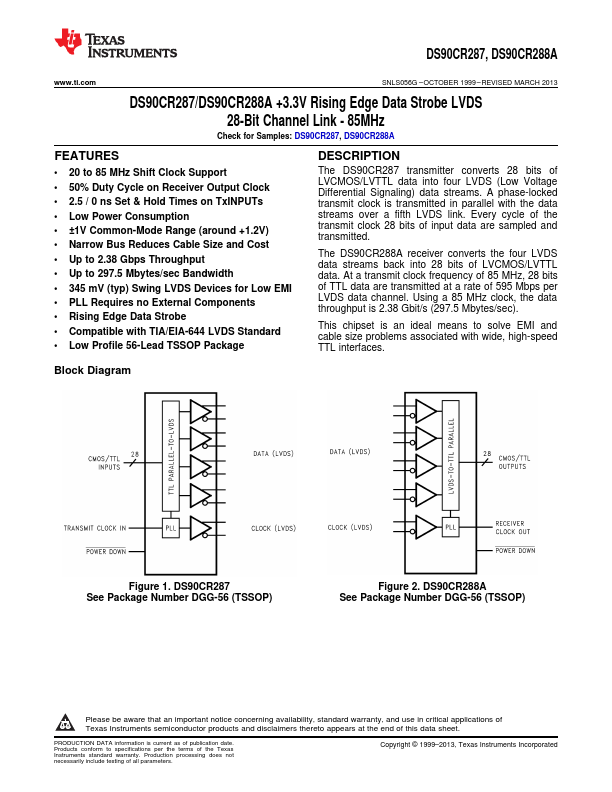
The DS90CR287 transmitter converts 28 bits of LV
CMOS/LVTTL data into four LVDS (Low
Voltage Differential Signaling) data streams. A phase-locked transmit clock is transmitted in parallel with the data streams over a fifth LVDS link. Every cycle of the transmit clock 28 bits of input data are sampled and transmitted.
The DS90CR288A receiver converts the four LVDS data streams back into 28 bits of LV
CMOS/LVTTL data. At a transmit clock frequency of 85 MHz, 28 bits of TTL data are transmitted at a rate of 595 Mbps per LVDS data channel. Using a 85 MHz clock, the data throughput is 2.38 Gbit/s (297.5 Mbytes/sec).
This chipset is an ideal means to solve EMI and cable size problems associated with wide, high-speed TTL interfaces.
Block Diagram
Figure 1. DS90CR287 See Package Number DGG...