8M x 32 / 2 x 8Mx 32 INTEL J3 BASED
www.DataSheet4U.com
White Electronic Designs
EDI7F328XDNSN EDI7F2328XDNSN
ADVANCED*
8M x 32 / 2 x 8Mx 32; INTEL J3 BA...
Description
www.DataSheet4U.com
White Electronic Designs
EDI7F328XDNSN EDI7F2328XDNSN
ADVANCED*
8M x 32 / 2 x 8Mx 32; INTEL J3 BASED, FLASH
FEATURES
8M x 32 and 2 x 8M x 32 Densities Based on Intel’s Strataflash (J3) family of Flash Devices E28F640J3 (64) 128Kb Erase Blocks (Symetrical) High Performance Interface Async Page Mode Reads 120/25 ns Read Access Time 2.7V - 3.6V Vcc Operation 128 bit Protection Register; 64 bit Unique Device Identifier 64 bit User Programmable OTP Cells Common Flash Interface (CFI) Scaleable Command Set (SCS) 32 byte Write Buffer, 64M Total Erase Cycles 100,000 Erase Cycles per Block Package 80 pin SIMM
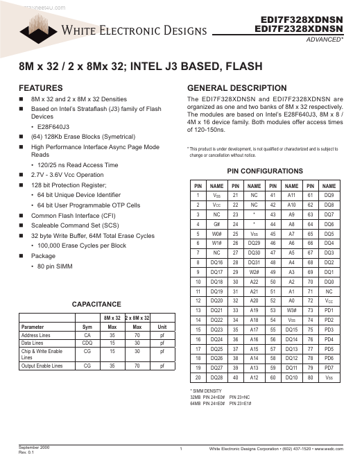
PIN 1 2 3 4 5 6 7 8 9 10 11 NAME VSS VCC NC G# W0# W1# NC DQ16 DQ17 DQ18 DQ19 DQ20 DQ21 DQ22 DQ23 DQ24 DQ25 DQ26 DQ27 DQ28
* This product is under development, is not qualified or characterized and is subject to change or cancellation without notice.
GENERAL DESCRIPTION
The EDI7F328XDNSN and EDI7F2328XDNSN are organized as one and two banks of 8M x 32 respectively. The modules are based on Intel’s E28F640J3, 8M x 8 / 4M x 16 device family. Both modules offer access times of 120-150ns.
PIN CONFIGURATIONS
PIN 21 22 23 24 25 26 27 28 29 30 31 32 33 34 35 36 37 38 39 40 NAME NC NC * * VSS DQ29 DQ30 DQ31 W2# A22 A21 A20 A19 A18 A17 A16 A15 A14 A13 A12 PIN 41 42 43 44 45 46 47 48 49 50 51 52 53 54 55 56 57 58 59 60 NAME A11 A10 A9 A8 A7 A6 A5 A4 A3 A2 A1 A0 W3# VSS DQ15 DQ14 DQ13 DQ12 DQ11 DQ10 PIN 61 62 63 64 65 66 67 68 69 70 71 72 73 74 75 76 77 78 7...
Similar Datasheet