www.DataSheet4U.com
EDI7F4341MC
4x1Mx32 FLASH MODULE
FEATURES
n 4x1Mx32 n Based on Intel's E28F008SA Flash Device n Fa...
www.DataSheet4U.com
EDI7F4341MC
4x1Mx32 FLASH MODULE
FEATURES
n 4x1Mx32 n Based on Intel's E28F008SA Flash Device n Fast Read Access Time - 90ns n 5- Volt-Only Reprogramming n Low Power Dissipation 60mA per Device Active Current 10µA per Device
CMOS Standby Current n Typical Endurance >100,000 Cycles n Single 5 Volt ±10% Supply n
CMOS and TTL Compatible Inputs and Outputs n Commercial and Industrial Temperature Range n Package 80 Pin SIMM (JEDEC)
DESCRIPTION
The EDI7F4341MC is organized as four banks of 1Mx32. The module is based on Intel's E28F008SA - 1Mx8 Flash device in TSOP packages which are mounted on an FR4 substrate. The module offers access times between 90 and 150ns allowing for operation of high-speed microprocessors without wait states.
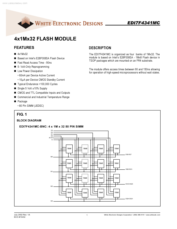
FIG. 1
BLOCK DIAGRAM EDI7F4341MC-BNC: 4 x 1M x 32 80 PIN SIMM
E3\ E2\ E1\ E0\ A0-A19 G\
1Mx8
1Mx8
1Mx8
1Mx8
DQ0-DQ7 W0\
1Mx8
1Mx8
1Mx8
1Mx8
DQ8-DQ15 W1\
1Mx8
1Mx8
1Mx8
1Mx8
DQ16-DQ23 W2\
1Mx8
1Mx8
1Mx8
1Mx8
DQ24-DQ31 W3\
July 2002 Rev. 1A ECO #15432
1
White Electronic Designs Corporation (508) 366-5151 www.whiteedc.com
EDI7F4341MC
CAPACITANCE
(f=1.0MHz, VIN = VCC or VSS) 4x1Meg Max 140 60 60 140
Parameter Address Lines Data lines Chip & Write Enable Lines Output Enable lines
Sym CA CDQ CC CG
Unit pF pF pF pF
PIN CONFIGURATIONS
Pin # 1 2 3 4 5 6 7 8 9 10 11 12 13 14 15 16 17 18 19 20 Pin Name VSS VCC VPP G\ W0\ W1\ NC DQ16 DQ17 DQ18 DQ19 DQ20 DQ21 DQ22 DQ23 DQ24 DQ25 DQ26 DQ27 DQ28 Pin # 21...