www.DataSheet4U.com
EMT1DXV6T1, EMT1DXV6T5 Dual General Purpose Transistor
PNP Dual
http://onsemi.com
This transistor ...
www.DataSheet4U.com
EMT1DXV6T1, EMT1DXV6T5 Dual General Purpose Transistor
PNP Dual
http://onsemi.com
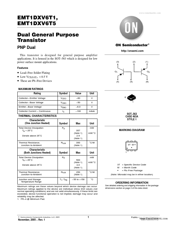
This transistor is designed for general purpose amplifier applications. It is housed in the SOT−563 which is designed for low power surface mount applications.
Features
(3)
(2)
(1)
Lead−Free Solder Plating Low VCE(SAT), t0.5 V These are Pb−Free Devices
MAXIMUM RATINGS
Rating Collector −Emitter
Voltage Collector −Base
Voltage Emitter −Base
Voltage Collector Current − Continuous Symbol VCEO VCBO VEBO IC Value −60 −50 −6.0 −100 Unit V V V mAdc
Q1
Q2
(4)
(5)
(6)
6 1
THERMAL CHARACTERISTICS
Characteristic (One Junction Heated) Total Device Dissipation TA = 25°C Derate above 25°C Thermal Resistance, Junction-to-Ambient Characteristic (Both Junctions Heated) Total Device Dissipation TA = 25°C Derate above 25°C Thermal Resistance, Junction-to-Ambient Junction and Storage Temperature Range RqJA TJ, Tstg RqJA Symbol PD 357 (Note 1) 2.9 (Note 1) 350 (Note 1) Max 500 (Note 1) 4.0 (Note 1) 250 (Note 1) −55 to +150 Max Unit mW
SOT−563 CASE 463A STYLE 1
MARKING DIAGRAM
mW/°C
°C/W
3T M G G 1
Symbol PD
Unit mW mW/°C
°C/W °C
3T = Specific Device Code M = Month Code G = Pb−Free Package (Note: Microdot may be in either location)
ORDERING INFORMATION
See detailed ordering and shipping information in the package dimensions section on page 2 of this data sheet.
Maximum ratings are those values beyond which device damage can occur. Maximum ratings applied to the device a...