FDC606P
FDC606P
P-Channel 1.8V Specified PowerTrench MOSFET
General Description
This P-Channel 1.8V specified MOSFET ...
FDC606P
FDC606P
P-Channel 1.8V Specified PowerTrench
MOSFET
General Description
This P-Channel 1.8V specified
MOSFET uses ON Semiconductor’s low
voltage PowerTrench process. It has been optimized for battery power management applications.
Applications
Battery management Load switch Battery protection
Features
–6 A, –12 V.
RDS(ON) = 26 mΩ @ VGS = –4.5 V RDS(ON) = 35 mΩ @ VGS = –2.5 V RDS(ON) = 53 mΩ @ VGS = –1.8 V
Fast switching speed
High performance trench technology for extremely low RDS(ON)
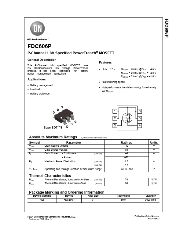
S D D
SuperSOT TM-6
G DD
1
6
2
5
3
4
Absolute Maximum Ratings TA=25oC unless otherwise noted
Symbol
VDSS
VGSS
ID
Parameter
Drain-Source
Voltage
Gate-Source
Voltage Drain Current – Continuous
– Pulsed
(Note 1a)
PD
Maximum Power Dissipation
(Note 1a) (Note 1b)
TJ, TSTG
Operating and Storage Junction Temperature Range
Thermal Characteristics
RθJA
Thermal Resistance, Junction-to-Ambient
RθJC
Thermal Resistance, Junction-to-Case
(Note 1a) (Note 1)
Package Marking and Ordering Information
Device Marking
Device
Reel Size
.606
FDC606P
7’’
Ratings
–12 ±8 –6 –20 1.6 0.8 –55 to +150
78 30
Tape width 8mm
Units
V V A
W
°C
°C/W °C/W
Quantity 3000 units
2001 Semiconductor Components Industries, LLC. September-2017, Rev. 5
Publication Order Number: FDC606P/D
FDC606P
Electrical Characteristics
Symbol
Parameter
TA = 25°C unless otherwise noted
Test Conditions
Min Typ Max Units
Off Characteristics
BVDSS
Drain–Source Breakdown
Voltage
∆BVDSS...