DATA SHEET www.onsemi.com
MOSFET – P-Channel, POWERTRENCH)
2.5 V Specified
FDC608PZ, FDC608PZ-F171
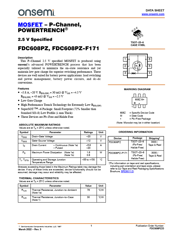
D DS
DG D TSOT−23−6...
DATA SHEET www.onsemi.com
MOSFET – P-Channel, POWERTRENCH)
2.5 V Specified
FDC608PZ, FDC608PZ-F171
D DS
DG D TSOT−23−6 CASE 419BL
Description This P−Channel 2.5 V specified
MOSFET is produced using
onsemi’s advanced POWERTRENCH process that has been especially tailored to minimize the on−state resistance and yet maintain low gate charge for superior switching performance. These devices are well suited for battery power applications: load switching and power management, battery power circuits, and dc−dc conversions.
Features
–5.8 A, –20 V. RDS(ON) = 30 mW @ VGS = –4.5 V
RDS(ON) = 43 mW @ VGS = –2.5 V
Low Gate Charge High Performance Trench Technology for Extremely Low RDS(ON) SuperSOT TM –6 Package: Small Footprint (72% Smaller than
Standard SO–8) Low Profile (1 mm Thick)
These Devices are Pb−Free and Halide Free
ABSOLUTE MAXIMUM RATINGS Values are at TA = 25°C unless otherwise noted.
Symbol
Parameter
Ratings Unit
VDSS Drain−Gate
Voltage
–20
V
VGSS Gate−Source
Voltage
±12
V
ID
Drain Current
– Continuous (Note 1a)
–5.8
A
– Pulsed
–20
PD
Maximum Power Dissipation (Note 1a)
(Note 1b)
1.6
W
0.8
TJ, TSTG Operating and Storage Junction Temperature Range
–55 to +150 °C
Stresses exceeding those listed in the Maximum Ratings table may damage the device. If any of these limits are exceeded, device functionality should not be assumed, damage may occur and reliability may be affected.
THERMAL CHARACTERISTICS Values are at TA = 25°C unless otherwise ...