Integrated Load Switch
FDC6323L
Description These Integrated Load Switches are produced using onsemi’s
proprietary, high...
Integrated Load Switch
FDC6323L
Description These Integrated Load Switches are produced using onsemi’s
proprietary, high cell density, DMOS technology. This very high density process is especially tailored to minimize on−state resistance and provide superior switching performance. These devices are particularly suited for low
voltage high side load switch application where low conduction loss and ease of driving are needed.
Features
VDROP = 0.2 V @ VIN = 5 V, IL = 1 A, VON/OFF = 1.5 V to 8 V VDROP = 0.3 V @ VIN = 3.3 V, IL = 1 A, VON/OFF = 1.5 V to 8 V High Density Cell Design for Extremely Low On−Resistance VON/OFF Zener Protection for ESD Ruggedness > 6 kV Human
Body Model
SUPERSOTt−6 Package Design Using Copper Lead Frame for
Superior Thermal and Electrical Capabilities
This is a Pb−Free and Halide Free Device
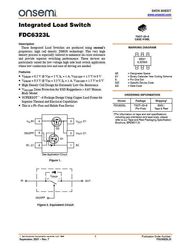
VIN,R1 4 ON/OFF 5
R1, C1 6
Q2 Q1
3 VOUT, C1 2 VOUT, C1 1 R1
See Application Circuit Figure 1.
DATA SHEET www.onsemi.com
TSOT−23−6 CASE 419BL
MARKING DIAGRAM
&E&Y &.323&G
&E
= Designates Space
&Y
= Binary Calendar Year Coding Scheme
&.
= Pin One Dot
323
= Specific Device Code
&G
= Date Code
ORDERING INFORMATION
Device FDC6323L
Package
TSOT−23−6 (Pb−Free)
Shipping†
3000 / Tape & Reel
†For information on tape and reel specifications, including part orientation and tape sizes, please refer to our Tape and Reel Packaging Specification Brochure, BRD8011/D.
VDROP
+
−
IN
OUT
ON/OFF Figure 2. Equivalent Circuit
© Semiconductor Componen...