MOSFET – P-Channel, POWERTRENCH
-20 V, -4 A, 100 mW
FDC642P-F085, FDC642P-F085P
Features
• Typ RDS(on) = 52.5 mW at VGS ...
MOSFET – P-Channel, POWERTRENCH
-20 V, -4 A, 100 mW
FDC642P-F085, FDC642P-F085P
Features
Typ RDS(on) = 52.5 mW at VGS = −4.5 V, ID = −4 A Typ RDS(on) = 75.3 mW at VGS = −2.5 V, ID = −3.2 A Fast Switching Speed Low Gate Charge (6.9 nC Typical) High Performance Trench Technology for Extremely Low RDS(on) SUPERSOTt−6 Package: Small Footprint (72% Smaller than
Standard SO−8); Low Profile (1 mm Thick)
AEC−Q101 Qualified and PPAP Capable This Device is Pb−Free and is RoHS Compliant
Applications
Load Switch Battery Protection Power management
www.onsemi.com
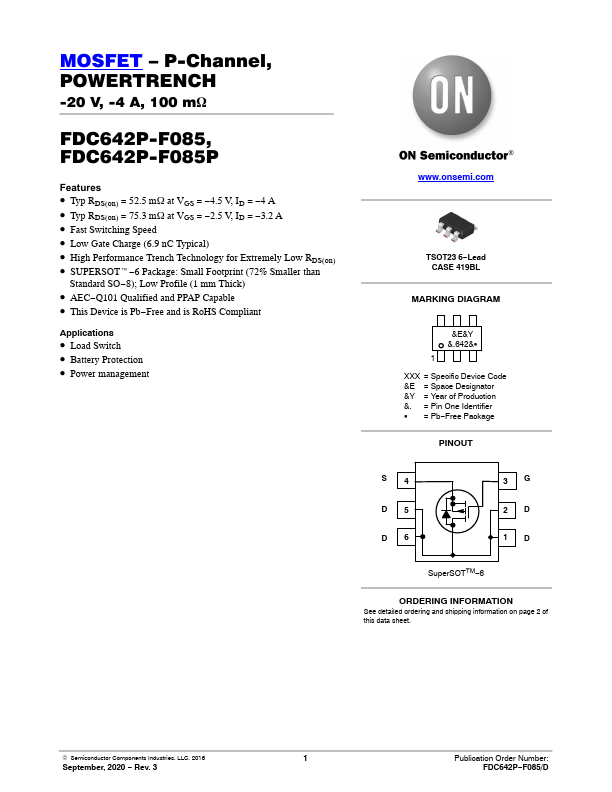
TSOT23 6−Lead CASE 419BL
MARKING DIAGRAM
&E&Y &.642&G 1 XXX = Specific Device Code &E = Space Designator &Y = Year of Production &. = Pin One Identifier G = Pb−Free Package
PINOUT
S4 D5 D6
3G 2D 1D
SuperSOTTM−6
ORDERING INFORMATION
See detailed ordering and shipping information on page 2 of this data sheet.
© Semiconductor Components Industries, LLC, 2016
1
September, 2020 − Rev. 3
Publication Order Number: FDC642P−F085/D
FDC642P−F085, FDC642P−F085P
MOSFET MAXIMUM RATINGS (TA = 25°C unless otherwise noted)
Symbol
Parameter
Ratings
Units
VDSS VGS ID
Drain to Source
Voltage
Gate to Source
Voltage
Drain Current − Continuous (VGS = 4.5 V) − Pulsed
−20
V
±8
V
A −4
−20
EAS
Single Pulse Avalanche Energy (Note 1)
PD
Power Dissipation
72
mJ
1.2
W
TJ, TSTG Operating and Storage Temperature
−55 to +150
°C
Stresses exceeding those listed in the Maximum Ratings table may damage the device...