MOSFET – Single, N-Channel, Logic Level, POWERTRENCH)
30 V, 6.3 A, 25 mW
FDC655BN
General Description This N−Channel Lo...
MOSFET – Single, N-Channel, Logic Level, POWERTRENCH)
30 V, 6.3 A, 25 mW
FDC655BN
General Description This N−Channel Logic Level
MOSFET is produced using onsemi’s
advanced POWERTRENCH process that has been especially tailored to minimize the on−state resistance and yet maintain superior switching performance.
These devices are well suited for low
voltage and battery powered applications where low in−line power loss and fast switching are required.
Features
Max RDS(ON) = 25 mW @ VGS = 10 V, ID = 6.3 A Max RDS(ON) = 33 mW @ VGS = 4.5 V, ID = 5.5 A Fast Switching Low Gate Charge High Performance Trench Technology for Extremely Low RDS(ON) This Device is Pb−Free, Halide Free and is RoHS Compliant
MOSFET MAXIMUM RATINGS (TC = 25°C, unless otherwise noted)
Symbol
Parameter
Value
Unit
VDS Drain to Source
Voltage
30
V
VGS Gate to Source
Voltage
±20
V
ID
−Continuous TA = 25°C (Note 1a)
6.3
A
−Pulsed
20
PD Power Dissipation
(Note 1a)
1.6
W
(Note 1b)
0.8
TJ, TSTG Operating and Storage Junction Temperature Range
−55 to +150 °C
Stresses exceeding those listed in the Maximum Ratings table may damage the device. If any of these limits are exceeded, device functionality should not be assumed, damage may occur and reliability may be affected.
THERMAL CHARACTERISTICS
Symbol
Parameter
Max
Unit
RqJA Thermal Resistance, Junction to Ambient
78 (Note 1a)
°C/W
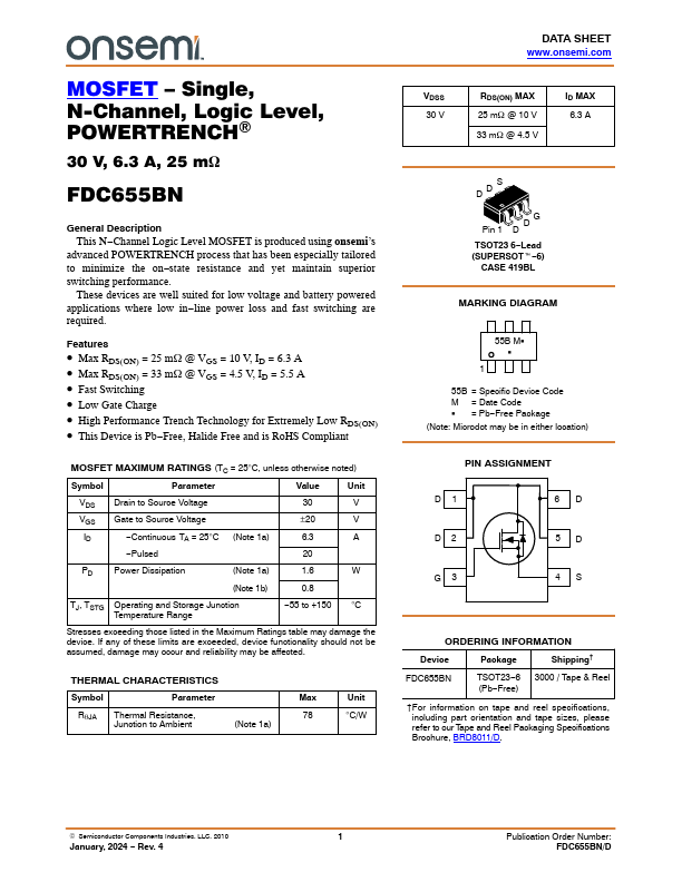
DATA SHEET www.onsemi.com
VDSS 30 V
RDS(ON) MAX 25 mW @ 10 V 33 mW @ 4.5 V
ID MAX 6.3 A
S...