FDD4685 40V P-Channel PowerTrench® MOSFET
March 2015
FDD4685 40V P-Channel PowerTrench® MOSFET
–40V, –32A, 27mΩ
Feat...
FDD4685 40V P-Channel PowerTrench®
MOSFET
March 2015
FDD4685 40V P-Channel PowerTrench®
MOSFET
–40V, –32A, 27mΩ
Features
General Description
Max rDS(on) = 27mΩ at VGS = –10V, ID = –8.4A Max rDS(on) = 35mΩ at VGS = –4.5V, ID = –7A High performance trench technology for extremely low rDS(on) RoHS Compliant
This P-Channel
MOSFET has been produced using Fairchild Semiconductor’s proprietary PowerTrench® technology to
deliver low rDS(on) and good switching characteristic offering superior performance in application.
Application
Inverter Power Supplies
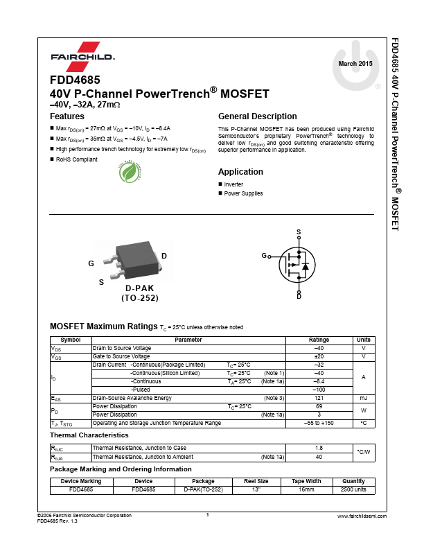
G S
D
DT O- P-2A5K2 (T O -25 2)
S G
D
MOSFET Maximum Ratings TC = 25°C unless otherwise noted
Symbol VDS VGS
ID
EAS PD TJ, TSTG
Parameter Drain to Source
Voltage Gate to Source
Voltage Drain Current -Continuous(Package Limited)
-Continuous(Silicon Limited) -Continuous -Pulsed Drain-Source Avalanche Energy Power Dissipation Power Dissipation Operating and Storage Junction Temperature Range
TC= 25°C TC= 25°C TA= 25°C
TC= 25°C
Thermal Characteristics
(Note 1) (Note 1a)
(Note 3)
(Note 1a)
Ratings –40 ±20 –32 –40 –8.4 –100 121 69 3
–55 to +150
Units V V
A
mJ W °C
RθJC RθJA
Thermal Resistance, Junction to Case Thermal Resistance, Junction to Ambient
Package Marking and Ordering Information
1.8
(Note 1a)
40
°C/W
Device Marking FDD4685
Device FDD4685
Package D-PAK(TO-252)
Reel Size 13’’
Tape Width 16mm
Quantity 2500 units
©2006 Fairchild Semiconductor Corporation
1
FDD4685 Rev. 1.3
www.fairchi...