MOSFET - P-Channel Logic Level PowerTrench)
-40 V, 13.5 mW, -50 A
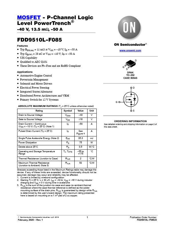
FDD9510L-F085
Features
• Typ RDS(on) = 11 mW at VGS =...
MOSFET - P-Channel Logic Level PowerTrench)
-40 V, 13.5 mW, -50 A
FDD9510L-F085
Features
Typ RDS(on) = 11 mW at VGS = −10 V; ID = −50 A Typ Qg(tot) = 28 nC at VGS = −10 V; ID = −50 A UIS Capability Qualified to AEC Q101 These Devices are Pb−Free and are RoHS Compliant
Applications
Automotive Engine Control Powertrain Management Solenoid and Motor Drivers Electrical Power Steering Integrated Starter/Alternator Distributed Power Architectures and VRM Primary Switch for 12 V Systems
ABSOLUTE MAXIMUM RATINGS (TJ = 25°C unless otherwise noted)
Rating
Symbol Value Unit
Drain to Source
Voltage
Gate to Source
Voltage
Drain Current − Continuous (VGS = −10 V) (TC = 25°C) (Note 1) Pulsed Drain Current (TC = 25°C)
VDSS
−40
V
VGS
±16
V
ID
−50
A
ID
See
A
Figure 4
Single Pulse Avalanche Energy (Note 2)
Power Dissipation Derate above 25°C
Operating and Storage Temperature Range
EAS PD PD TJ, TSTG
35.3
75
0.5
−55 to +175
mJ W W/°C °C
Thermal Resistance (Junction to Case)
Maximum Thermal Resistance (Junction to Ambient) (Note 3)
RqJC RqJA
2
°C/W
52
°C/W
Stresses exceeding those listed in the Maximum Ratings table may damage the device. If any of these limits are exceeded, device functionality should not be assumed, damage may occur and reliability may be affected. 1. Current is limited by wirebond configuration 2. Starting Tj = 25°C, L = 40 mH, IAS = −42 A, VDD = −40 V during inductor
charging and VDD = 0 V during time in avalanche 3. RqJA ...