Dual N-Channel, Digital FET
FDG6301N-F085
Features
• 25 V, 0.22 A Continuous, 0.65 A Peak • RDS(ON) = 4 Ω @ VGS = 4.5 ...
Dual N-Channel, Digital FET
FDG6301N-F085
Features
25 V, 0.22 A Continuous, 0.65 A Peak RDS(ON) = 4 Ω @ VGS = 4.5 V, RDS(ON) = 5 Ω @ VGS = 2.7 V. Very Low Level Gate Drive Requirements allowing Directop−
Eration in 3 V Circuits (VGS(th) < 1.5 V)
Gate−Source Zener for ESD Ruggedness ( >6 kV Human Body
Model)
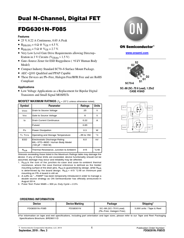
Compact Industry Standard SC70−6 Surface Mount Package. AEC−Q101 Qualified and PPAP Capable These Devices are Pb−Free, Halogen Free/BFR Free and are RoHS
Compliant
Applications
Low
Voltage Applications as a Replacement for Bipolar Digital
Transistors and Small Signal
MOSFETs
MOSFET MAXIMUM RATINGS (TA = 25°C unless otherwise noted)
Symbol
Parameter
Ratings Units
VDSS Drain to Source
Voltage
25 V
VGS Gate to Source
Voltage
8V
ID Drain Current Continuous
0.22 A
Pulsed
0.65
PD Power Dissipation
0.3 W
TJ, TSTG ESD
Operating and Storage Temperature
Electrostatic Discharge Rating MIL−STD−883D Human Body Model (100 pF / 1500 W)
−55 to 150 6.0
°C kV
RqJA Thermal Resistance, Junction to Ambient 415 °C/W
Stresses exceeding those listed in the Maximum Ratings table may damage the device. If any of these limits are exceeded, device functionality should not be assumed, damage may occur and reliability may be affected. 1. RθJA is the sum of the junction−to−case and case−to−ambient thermal
resistance, where the case thermal reference is defined as the Solder mounting surface of the drain pins. RθJC is guaranteed by design, while RθJA is determined ...