Digital FET, Dual N-Channel
FDG6303N
General Description These dual N−Channel logic level enhancement mode field effec...
Digital FET, Dual N-Channel
FDG6303N
General Description These dual N−Channel logic level enhancement mode field effect
transistors are produced using ON Semiconductor’s proprietary, high cell density, DMOS technology. This very high density process is especially tailored to minimize on−state resistance. This device has been designed especially for low
voltage applications as a replacement for bipolar digital transistors and small signal
MOSFETs.
Features
25 V, 0.50 A Continuous, 1.5 A Peak
♦ RDS(ON) = 0.45 W @ VGS = 4.5 V ♦ RDS(ON) = 0.60 W @ VGS = 2.7 V
Very Low Level Gate Drive Requirements Allowing Direct
Operation in 3 V Circuits (VGS(th) < 1.5 V)
Gate−Source Zener for ESD Ruggedness (>6 kV Human Body
Model)
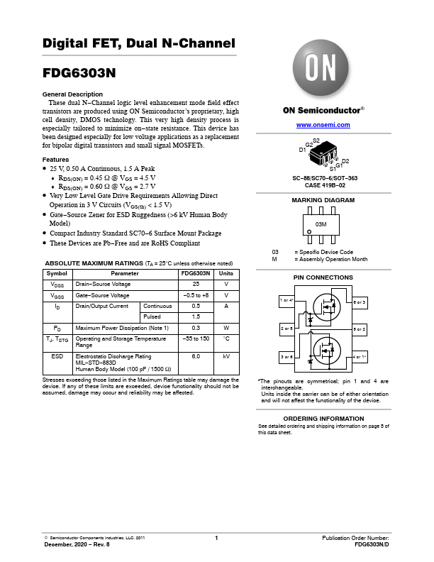
Compact Industry Standard SC70−6 Surface Mount Package These Devices are Pb−Free and are RoHS Compliant
ABSOLUTE MAXIMUM RATINGS (TA = 25°C unless otherwise noted)
Symbol
Parameter
FDG6303N Units
VDSS Drain−Source
Voltage
25
V
VGSS Gate−Source
Voltage
−0.5 to +8
V
ID
Drain/Output Current
Continuous
0.5
A
Pulsed
1.5
PD
Maximum Power Dissipation (Note 1)
0.3
W
TJ, TSTG Operating and Storage Temperature Range
−55 to 150 °C
ESD Electrostatic Discharge Rating
6.0
kV
MIL−STD−883D
Human Body Model (100 pF / 1500 W)
Stresses exceeding those listed in the Maximum Ratings table may damage the device. If any of these limits are exceeded, device functionality should not be assumed, damage may occur and reliability may be affected.
www.on...