FDG6308P
January 2001
FDG6308P
P-Channel 1.8V Specified PowerTrench MOSFET
General Description
This P-Channel 1.8V s...
FDG6308P
January 2001
FDG6308P
P-Channel 1.8V Specified PowerTrench
MOSFET
General Description
This P-Channel 1.8V specified
MOSFET uses Fairchild’s advanced low
voltage PowerTrench process. It has been optimized for battery power management applications.
Applications
Battery management Load switch
Features
–0.6 A, –20 V.
RDS(ON) = 0.40 Ω @ VGS = –4.5 V RDS(ON) = 0.55 Ω @ VGS = –2.5 V RDS(ON) = 0.80 Ω @ VGS = –1.8 V
Low gate charge
High performance trench technology for extremely low RDS(ON)
Compact industry standard SC70-6 surface mount package
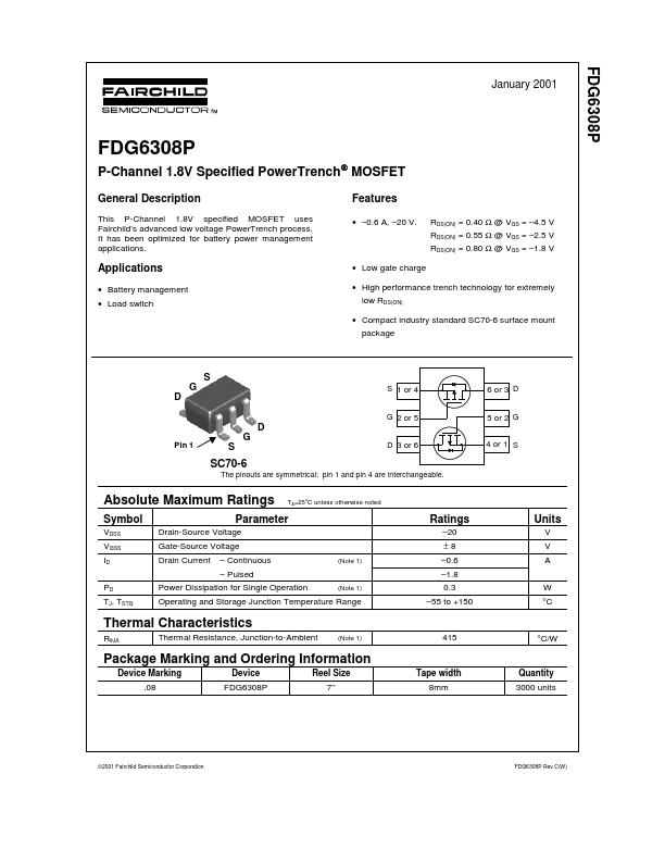
S G D
S 1 or 4
Pin 1
D G S
G 2 or 5 D 3 or 6
SC70-6
The pinouts are symmetrical; pin 1 and pin 4 are interchangeable.
6 or 3 D 5 or 2 G 4 or 1 S
Absolute Maximum Ratings TA=25oC unless otherwise noted
Symbol
Parameter
VDSS VGSS ID
Drain-Source
Voltage Gate-Source
Voltage Drain Current – Continuous
– Pulsed
(Note 1)
PD TJ, TSTG
Power Dissipation for Single Operation
(Note 1)
Operating and Storage Junction Temperature Range
Thermal Characteristics
RθJA
Thermal Resistance, Junction-to-Ambient
(Note 1)
Package Marking and Ordering Information
Device Marking
Device
Reel Size
.08
FDG6308P
7’’
Ratings
–20 ±8 –0.6 –1.8 0.3 –55 to +150
415
Tape width 8mm
Units
V V A
W °C
°C/W
Quantity 3000 units
2001 Fairchild Semiconductor Corporation
FDG6308P Rev C(W)
FDG6308P
Electrical Characteristics
Symbol
Parameter
TA = 25°C unless otherwise noted
Test Conditions
Min Typ Max Units
Off Charact...