FDG6318PZ
January 2003
FDG6318PZ
Dual P-Channel, Digital FET
General Description
These dual P-Channel logic level enha...
FDG6318PZ
January 2003
FDG6318PZ
Dual P-Channel, Digital FET
General Description
These dual P-Channel logic level enhancement mode
MOSFET are produced using Fairchild Semiconductor’s especially tailored to minimize on-state resistance. This device has been designed especially for bipolar digital transistors and small signal
MOSFETS
Features
-0.5A, -20V. r DS(ON) = 780mΩ (Max)@ VGS = -4.5 V rDS(ON) = 1200mΩ (Max) @ V GS = -2.5 V
Very low level gate drive requirements allowing direct operation in 3V circuits (V GS(TH) < 1.5V). Gate-Source Zener for ESD ruggedness (>1.4kV Human Body Model). Compact industry standard SC-70-6 surface mount package.
Applications
Battery management
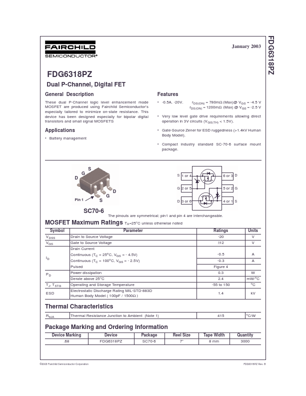
S G D D G
Pin 1
S 1 or 4
6 or 3 D 5 or 2 G 4 or 1 S
G 2 or 5
S
D 3 or 6
SC70-6
Symbol VDSS VGS
The pinouts are symmetrical; pin1 and pin 4 are interchangeable.
MOSFET Maximum Ratings TA=25°C unless otherwise noted
Parameter Drain to Source
Voltage Gate to Source
Voltage Drain Current ID Continuous (TC = 25oC, VGS = - 4.5V) Continuous (TC = 100 C, VGS = - 2.5V) Pulsed PD TJ, TSTG ESD Power dissipation Derate above 25°C Operating and Storage Temperature Electrostatic Discharge Rating MIL-STD-883D Human Body Model ( 100pF / 1500Ω )
o
Ratings -20 ±12 -0.5 -0.3 Figure 4 0.3 2.4 -55 to 150 1.4
Units V V A A W mW/oC
o
C
kV
Thermal Characteristics
Rθ JA Thermal Resistance Junction to Ambient (Note 1) 415
o
C/W
Package Marking and Ordering Information
Device Marking .68 Device FDG6318...