FDB33N25 / FDI33N25 250V N-Channel MOSFET
FDB33N25 / FDI33N25
250V N-Channel MOSFET Features
• 33A, 250V, RDS(on) = 0.0...
FDB33N25 / FDI33N25 250V N-Channel
MOSFET
FDB33N25 / FDI33N25
250V N-Channel
MOSFET Features
33A, 250V, RDS(on) = 0.094Ω @VGS = 10 V Low gate charge ( typical 36.8 nC) Low Crss ( typical 39 pF) Fast switching 100% avalanche tested Improved dv/dt capability
UniFET
Description
May 2006
TM
These N-Channel enhancement mode power field effect transistors are produced using Fairchild’s proprietary, planar stripe, DMOS technology. This advanced technology has been especially tailored to minimize on-state resistance, provide superior switching performance, and withstand high energy pulse in the avalanche and commutation mode. These devices are well suited for high efficient switched mode power supplies and active power factor correction.
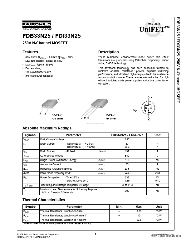
D
D
G G S
D -PAK
FDB Series
2
G D S
www.DataSheet4U.com
I -PAK
FDI Series
2
S
Absolute Maximum Ratings
Symbol
VDSS ID IDM VGSS EAS IAR EAR dv/dt PD TJ, TSTG TL Drain-Source
Voltage Drain Current Drain Current Gate-Source
voltage Single Pulsed Avalanche Energy Avalanche Current Repetitive Avalanche Energy Peak Diode Recovery dv/dt Power Dissipation (TC = 25°C) - Derate above 25°C
(Note 2) (Note 1) (Note 1) (Note 3)
Parameter
- Continuous (TC = 25°C) - Continuous (TC = 100°C) - Pulsed
(Note 1)
FDB33N25 / FDI33N25
250 33 20.4 132 ±30 918 33 23.5 4.5 235 1.89 -55 to +150 300
Unit
V A A A V mJ A mJ V/ns W W/°C °C °C
Operating and Storage Temperature Range Maximum Lead Temperature for Soldering Purpose, 1/8” from Case for 5 S...