1N/FDLL 914/A/B / 916/A/B / 4148 / 4448
Discrete POWER & Signal Technologies
1N/FDLL 914/A/B / 916/A/B / 4148 / 4448
C...
1N/FDLL 914/A/B / 916/A/B / 4148 / 4448
Discrete POWER & Signal Technologies
1N/FDLL 914/A/B / 916/A/B / 4148 / 4448
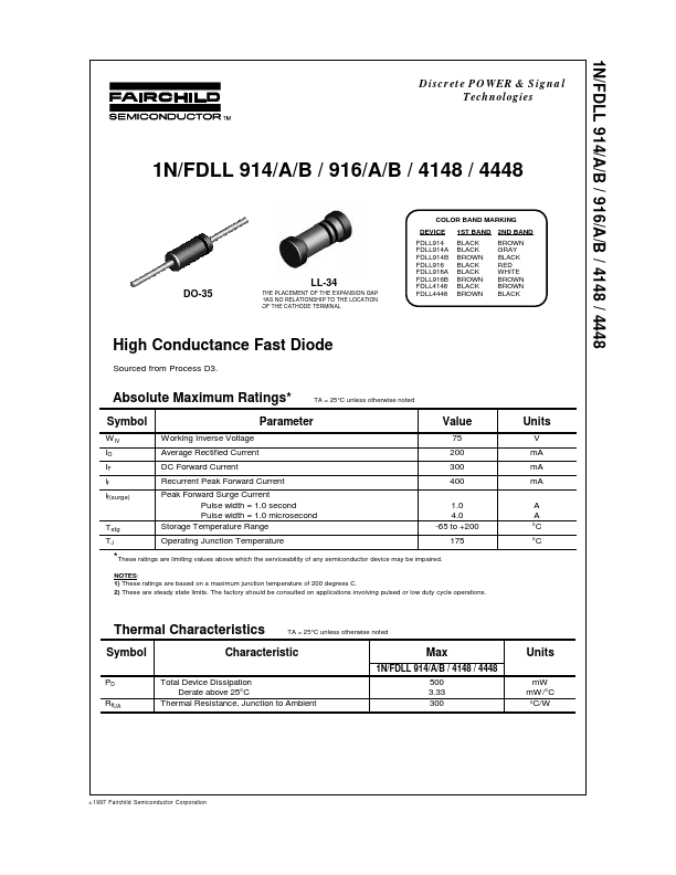
COLOR BAND MARKING DEVICE FDLL914 FDLL914A FDLL914B FDLL916 FDLL916A FDLL916B FDLL4148 FDLL4448 1ST BAND 2ND BAND BLACK BLACK BROWN BLACK BLACK BROWN BLACK BROWN BROWN GRAY BLACK RED WHITE BROWN BROWN BLACK
LL-34 DO-35
THE PLACEMENT OF THE EXPANSION GAP HAS NO RELATIONSHIP TO THE LOCATION OF THE CATHODE TERMINAL
High Conductance Fast Diode
Sourced from Process D3.
Absolute Maximum Ratings*
Symbol
W IV IO IF if if(surge) Working Inverse
Voltage Average Rectified Current DC Forward Current Recurrent Peak Forward Current
TA = 25°C unless otherwise noted
Parameter
Value
75 200 300 400 1.0 4.0 -65 to +200 175
Units
V mA mA mA A A °C °C
Tstg TJ
Peak Forward Surge Current Pulse width = 1.0 second Pulse width = 1.0 microsecond Storage Temperature Range Operating Junction Temperature
*These ratings are limiting values above which the serviceability of any semiconductor device may be impaired.
NOTES: 1) These ratings are based on a maximum junction temperature of 200 degrees C. 2) These are steady state limits. The factory should be consulted on applications involving pulsed or low duty cycle operations.
Thermal Characteristics
Symbol
PD RθJA
TA = 25°C unless otherwise noted
Characteristic
Total Device Dissipation Derate above 25°C Thermal Resistance, Junction to Ambient
Max
1N/FDLL 914/A/B / 4148 / 4448 500 3.33 300
Units
mW mW/°C °C/W
ã 1997 Fairchild...