MOSFET – N-Channel, POWERTRENCH)
100 V, 4.4 A, 60 mW
FDM3622
General Description This N−Channel MOSFET is produced using...
MOSFET – N-Channel, POWERTRENCH)
100 V, 4.4 A, 60 mW
FDM3622
General Description This N−Channel
MOSFET is produced using onsemi’s advanced
POWERTRENCH process that has been especially tailored to minimize the on−state resistance and yet maintain low gate charge for superior switching performance.
Features
Max rDS(on) = 60 mW at VGS = 10 V, ID = 4.4 A Max rDS(on) = 80 mW at VGS = 6.0 V, ID = 3.8 A Low Miller Charge Low QRR Body Diode Optimized efficiency at high frequencies UIS Capability (Single Pulse and Repetitive Pulse) This Device is Pb−Free, Halide Free and is RoHS Compliant
MOSFET MAXIMUM RATINGS (TA = 25°C, unless otherwise noted)
Symbol
Parameter
Ratings Unit
VDS Drain to Source
Voltage
VGS Gate to Source
Voltage
ID
Drain Current
− Continuous (Note 1a)
− Pulsed
100
V
±20
V
A 4.4 20
EAS Single Pulse Avalanche Energy (Note 3)
54
mJ
PD Power Dissipation (Note 1a)
(Note 1b)
W 2.1 0.9
TJ, TSTG Operating and Storage Junction Temperature Range
−55 to +150 °C
Stresses exceeding those listed in the Maximum Ratings table may damage the device. If any of these limits are exceeded, device functionality should not be assumed, damage may occur and reliability may be affected.
THERMAL CHARACTERISTICS (TA = 25°C, unless otherwise noted)
Symbol
Parameter
Ratings Unit
RqJC Thermal Resistance, Junction to Case (Note 1)
3.0
°C/W
RqJA Thermal Resistance, Junction to Ambient
60
(Note 1a)
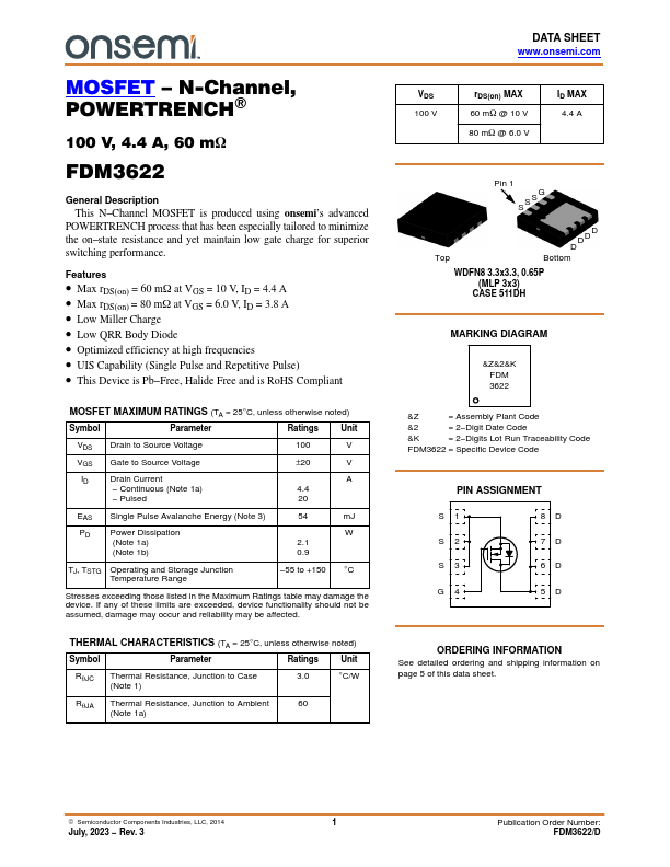
DATA SHEET www.onsemi.com
VDS 100 V
rDS(on) MAX 60 mW...