FDMA6023PZT Dual P-Channel PowerTrench® MOSFET
FDMA6023PZT
Dual P-Channel PowerTrench® MOSFET
-20 V, -3.6 A, 60 mΩ
F...
FDMA6023PZT Dual P-Channel PowerTrench®
MOSFET
FDMA6023PZT
Dual P-Channel PowerTrench®
MOSFET
-20 V, -3.6 A, 60 mΩ
Features
Max rDS(on) = 60 mΩ at VGS = -4.5 V, ID = -3.6 A Max rDS(on) = 80 mΩ at VGS = -2.5 V, ID = -3.0 A Max rDS(on) = 110 mΩ at VGS = -1.8 V, ID = -2.0 A Max rDS(on) = 170 mΩ at VGS = -1.5 V, ID = -1.0 A Low Profile-0.55 mm maximum - in the new
package MicroFET 2x2 mm Thin HBM ESD protection level > 2.4 kV typical (Note 3)
RoHS Compliant
Free from halogenated compounds and antimony oxides
General Description
This device is designed specifically as a single package solution for the battery charge switch in cellular handset and other ultraportable applications. It features two independent P-Channel
MOSFETs with low on-state resistance for minimum conduction losses. When connected in the typical common source configuration, bi-directional current flow is possible.
The MicroFET 2X2 Thin package offers exceptional thermal performance for it’s physical size and is well suited to linear mode applications.
Applications
Battery protection
Battery management
Load switch
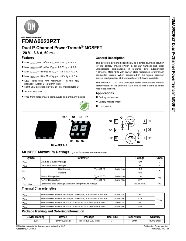
Pin 1 S1 G1 D2 D1 D2
Q1 S1 1
G1 2
6 D1 5 G2
D1 G2 S2 MicroFET 2x2
D2 3
4 S2 Q2
MOSFET Maximum Ratings TA = 25 °C unless otherwise noted
Symbol VDS VGS ID
PD TJ, TSTG
Parameter
Drain to Source
Voltage
Gate to Source
Voltage
-Continuous -Pulsed
TA = 25 °C
Power Dissipation
TA = 25 °C
Power Dissipation
TA = 25 °C
Operating and Storage Junction Temperature Range...