www.DataSheet4U.com
FDMC6890NZ Dual N-Channel PowerTrench® MOSFET
October 2006
FDMC6890NZ Dual N-Channel PowerTrench®...
www.DataSheet4U.com
FDMC6890NZ Dual N-Channel PowerTrench®
MOSFET
October 2006
FDMC6890NZ Dual N-Channel PowerTrench®
MOSFET
20V, 4A, Q1:68mΩ, Q2:100mΩ Features
Q1: N-Channel Max rDS(on) = 68mΩ at VGS = 4.5V, ID = 4A Max rDS(on) = 100mΩ at VGS = 2.5V, ID = 3A Q2: N-Channel Max rDS(on) = 100mΩ at VGS = 4.5V, ID = 4A Max rDS(on) = 150mΩ at VGS = 2.5V, ID = 2A Low gate Charge RoHS Compliant
tm
General Description
FDMC6890NZ is a compact single package solution for DC to DC converters with excellent thermal and switching characteristics. Inside the Power 33 package features two N-channel
MOSFETs with low on-state resistance and low gate charge to maximize the power conversion and switching efficiency. The Q1 switch also integrates gate protection from unclamped
voltage input.
Application
DC - DC Conversion
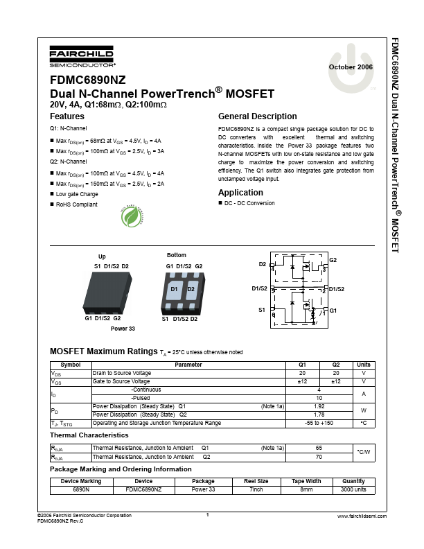
Up S1 D1/S2 D2
Bottom G1 D1/S2 G2 D2 4 3
G2
D1
D2
D1/S2 5 S1
2 D1/S2 G1
G1 D1/S2 G2 Power 33
S1 D1/S2 D2
6
1
MOSFET Maximum Ratings TA = 25°C unless otherwise noted
Symbol VDS VGS ID PD TJ, TSTG Parameter Drain to Source
Voltage Gate to Source
Voltage -Continuous -Pulsed Power Dissipation (Steady State) Q1 Power Dissipation (Steady State) Q2 Operating and Storage Junction Temperature Range (Note 1a) Q1 20 ±12 4 10 1.92 1.78 -55 to +150 Q2 20 ±12 Units V V A W °C
Thermal Characteristics
RθJA RθJA Thermal Resistance, Junction to Ambient Thermal Resistance, Junction to Ambient Q1 Q2 (Note 1a) 65 70 °C/W
Package Marking and Ordering Information
Dev...