MOSFET, N-Channel, POWERTRENCH)
Q1: 30 V, 66 A, 4 mW Q2: 30 V, 42 A, 5.5 mW
FDMD8900
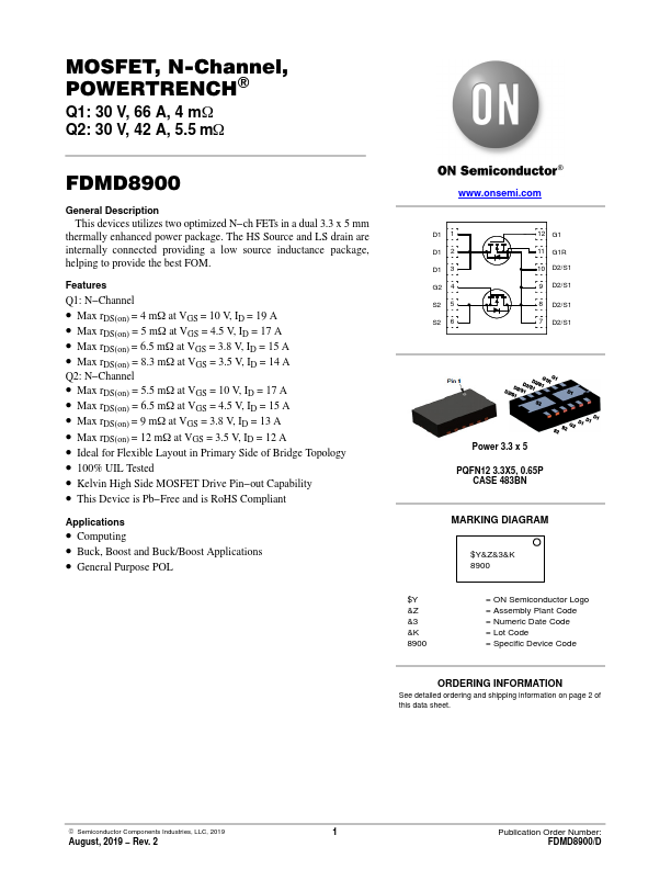
General Description This devices u...
MOSFET, N-Channel, POWERTRENCH)
Q1: 30 V, 66 A, 4 mW Q2: 30 V, 42 A, 5.5 mW
FDMD8900
General Description This devices utilizes two optimized N−ch FETs in a dual 3.3 x 5 mm
thermally enhanced power package. The HS Source and LS drain are internally connected providing a low source inductance package, helping to provide the best FOM.
Features
Q1: N−Channel
Max rDS(on) = 4 mW at VGS = 10 V, ID = 19 A Max rDS(on) = 5 mW at VGS = 4.5 V, ID = 17 A Max rDS(on) = 6.5 mW at VGS = 3.8 V, ID = 15 A Max rDS(on) = 8.3 mW at VGS = 3.5 V, ID = 14 A
Q2: N−Channel
Max rDS(on) = 5.5 mW at VGS = 10 V, ID = 17 A Max rDS(on) = 6.5 mW at VGS = 4.5 V, ID = 15 A Max rDS(on) = 9 mW at VGS = 3.8 V, ID = 13 A Max rDS(on) = 12 mW at VGS = 3.5 V, ID = 12 A Ideal for Flexible Layout in Primary Side of Bridge Topology 100% UIL Tested Kelvin High Side
MOSFET Drive Pin−out Capability This Device is Pb−Free and is RoHS Compliant
Applications
Computing Buck, Boost and Buck/Boost Applications General Purpose POL
www.onsemi.com
D1 1 D1 2 D1 3 G2 4 S2 5 S2 6
12 G1 11 G1R 10 D2/S1 9 D2/S1 8 D2/S1 7 D2/S1
Power 3.3 x 5
PQFN12 3.3X5, 0.65P CASE 483BN
MARKING DIAGRAM
$Y&Z&3&K 8900
$Y &Z &3 &K 8900
= ON Semiconductor Logo = Assembly Plant Code = Numeric Date Code = Lot Code = Specific Device Code
ORDERING INFORMATION
See detailed ordering and shipping information on page 2 of this data sheet.
© Semiconductor Components Industries, LLC, 2019
1
August, 2019 − Rev. 2
Publicatio...