FDMQ8203 Dual N-Channel and Dual P-Channel PowerTrench® MOSFET
FDMQ8203
December 2011
GreenBridgeTM Series of High-Ef...
FDMQ8203 Dual N-Channel and Dual P-Channel PowerTrench®
MOSFET
FDMQ8203
December 2011
GreenBridgeTM Series of High-Efficiency Bridge Rectifiers Dual N-Channel and Dual P-Channel PowerTrench®
MOSFET
N-Channel: 100 V, 6 A, 110 mΩ P-Channel: -80 V, -6 A, 190 mΩ
Features
General Description
Q1/Q4: N-Channel Max rDS(on) = 110 mΩ at VGS = 10 V, ID = 3 A Max rDS(on) = 175 mΩ at VGS = 6 V, ID = 2.4 A
Q2/Q3: P-Channel Max rDS(on) = 190 mΩ at VGS = -10 V, ID = -2.3 A Max rDS(on) = 235 mΩ at VGS = -4.5 V, ID = -2.1 A Substantial efficiency benefit in PD solutions
RoHS Compliant
This quad
mosfet solution provides ten-fold improvement in power dissipation over diode bridge.
Application
High-Efficiency Bridge Rectifiers
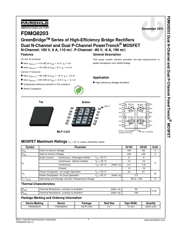
Top
G4 S4 S4 G3 S3 S3
Bottom
D3/ D1/ D4 D2
D3/ D1/ D4 D2
G1 S1 S1 G2 S2 S2
Pin 1
MLP 4.5x5
S3 7 S3 8
Q3 (Pch) Q2 (Pch)
6 S2 5 S2
G3 9
4 G2
S4 10 S4 11
Q4 (Nch)
Q1 (Nch)
3 S1 2 S1
G4 12
1 G1
D3,D4 to backside (isolated from D1,D2)
D1,D2 to backside
MOSFET Maximum Ratings TA = 25 °C unless otherwise noted
Symbol VDS VGS
ID
PD TJ, TSTG
Parameter
Drain to Source
Voltage
Gate to Source
Voltage
Drain Current
-Continuous (Package limited) -Continuous (Silicon limited) -Continuous -Pulsed
TC = 25 °C TC = 25 °C TA = 25 °C
Power Dissipation for Single Operation
TC = 25 °C
Power Dissipation for Dual Operation
TA = 25 °C
Operating and Storage Junction Temperature Range
Thermal Characteristics
(Note 1a) (Note 1a)
Q1/Q4
Q2/Q3
100...