FDMS86540 N-Channel PowerTrench® MOSFET
FDMS86540
N-Channel PowerTrench® MOSFET
60 V, 129 A, 3.4 mΩ
Features
Max rDS(...
FDMS86540 N-Channel PowerTrench®
MOSFET
FDMS86540
N-Channel PowerTrench®
MOSFET
60 V, 129 A, 3.4 mΩ
Features
Max rDS(on) = 3.4 mΩ at VGS = 10 V, ID = 20 A Max rDS(on) = 4.1 mΩ at VGS = 8 V, ID = 18.5 A Advanced Package and Silicon combination for low rDS(on)
and high efficiency
Next generation enhanced body diode technology, engineered for soft recovery
MSL1 robust package design
100% UIL tested
RoHS Compliant
May 2015
General Description
This N-Channel
MOSFET has been designed specifically to improve the overall efficiency and to minimize switch node ringing of DC/DC converters using either synchronous or conventional switching PWM controllers.It has been optimized for low gate charge, low rDS(on), fast switching speed and body diode reverse recovery performance.
Applications
Primary Switch in isolated DC-DC Synchronous Rectifier Load Switch
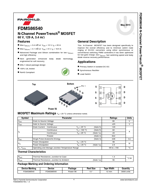
Top
Bottom
Pin 1 S
S
D
S
S G
S
D
Power 56
D D D D
MOSFET Maximum Ratings TA = 25 °C unless otherwise noted.
Symbol VDS VGS
ID
EAS PD TJ, TSTG
Parameter
Drain to Source
Voltage
Gate to Source
Voltage
Drain Current -Continuous -Continuous -Continuous -Pulsed
TC = 25 °C TC = 100 °C TA = 25 °C
Single Pulse Avalanche Energy
Power Dissipation
TC = 25 °C
Power Dissipation
TA = 25 °C
Operating and Storage Junction Temperature Range
Thermal Characteristics
S G
(Note 5) (Note 5) (Note 1a) (Note 4) (Note 3) (Note 1a)
D D
Ratings 60 ±20 129 82 20 642 228 96 2.5
-55 to +150
Units V V
A
mJ W °C
RθJC ...