www.DataSheet.co.kr
FDMS8662 N-Channel PowerTrench® MOSFET
November 2007
FDMS8662
N-Channel PowerTrench MOSFET
30V, 4...
www.DataSheet.co.kr
FDMS8662 N-Channel PowerTrench®
MOSFET
November 2007
FDMS8662
N-Channel PowerTrench
MOSFET
30V, 49A, 2.0mΩ
Features
Max rDS(on) = 2.0mΩ at VGS = 10V, ID = 28A Max rDS(on) = 3.0mΩ at VGS = 4.5V, ID = 24A Advanced Package and Silicon combination for low rDS(on) and high efficiency MSL1 robust package design RoHS Compliant
®
tm
General Description
The FDMS8662 has been designed to minimize losses in power conversion application. Advancements in both silicon and package technologies have been combined to offer the lowest rDS(on) while maintaining excellent switching performance.
Applications
Low Side for Synchronous Buck to Power Core Processor Secondary Side Synchronous Rectifier Low Side Switch in POL DC/DC Converter Oring FET/ Load Switch
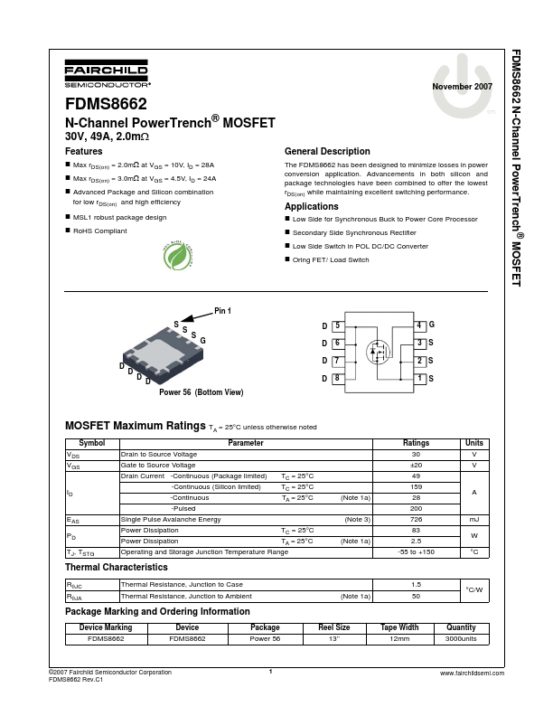
Pin 1 S S D S G D D D D D Power 56 (Bottom View) D 5 6 7 8 4 G
3 S 2 S 1 S
D
MOSFET Maximum Ratings TA = 25°C unless otherwise noted
Symbol VDS VGS Parameter Drain to Source
Voltage Gate to Source
Voltage Drain Current -Continuous (Package limited) ID -Continuous (Silicon limited) -Continuous -Pulsed EAS PD TJ, TSTG Single Pulse Avalanche Energy Power Dissipation Power Dissipation TC = 25°C TA = 25°C (Note 1a) (Note 3) TC = 25°C TC = 25°C TA = 25°C (Note 1a) Ratings 30 ±20 49 159 28 200 726 83 2.5 -55 to +150 mJ W °C A Units V V
Operating and Storage Junction Temperature Range
Thermal Characteristics
RθJC RθJA Thermal Resistance, Junction to Case Thermal Resistance, Junction to Ambient (Note ...