FDMS8672S N-Channel PowerTrench® SyncFETTM
February 2007
FDMS8672S N-Channel PowerTrench® SyncFETTM
30V, 35A, 5mΩ Feat...
FDMS8672S N-Channel PowerTrench® SyncFETTM
February 2007
FDMS8672S N-Channel PowerTrench® SyncFETTM
30V, 35A, 5mΩ Features General Description
Max rDS(on) = 5.0mΩ at VGS = 10V, ID = 17A Max rDS(on) = 7.0mΩ at VGS = 4.5V, ID = 15A Advanced Package and Silicon combination for low rDS(on) and high efficiency SyncFET Schottky Body Diode MSL1 robust package design RoHS Compliant
tm
The FDMS8672S has been designed to minimize losses in power conversion application. Advancements in both silicon and package technologies have been combined to offer the lowest rDS(on) while maintaining excellent switching performance. This device has the added benefit of an efficient monolithic Schottky body diode.
Application
Synchronous Rectifier for DC/DC Converters Notebook Vcore/ GPU low side switch Networking Point of Load low side switch Telecom secondary side rectification
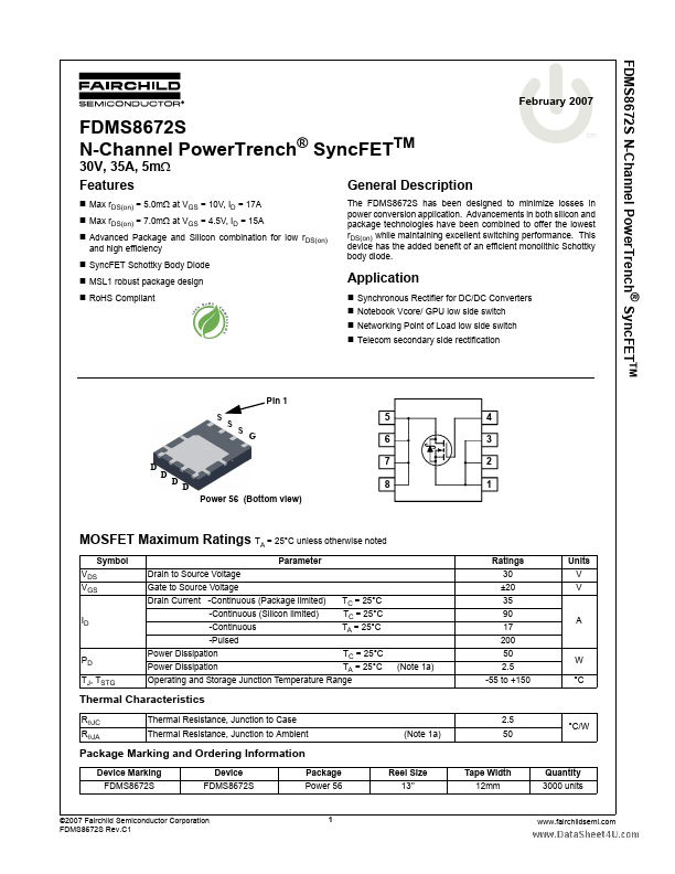
Pin 1 S S
5
S G
www.DataSheet4U.com
4 3 2 1
6 7
D
D
D
D Power 56 (Bottom view)
8
MOSFET Maximum Ratings TA = 25°C unless otherwise noted
Symbol VDS VGS ID Parameter Drain to Source
Voltage Gate to Source
Voltage Drain Current -Continuous (Package limited) -Continuous (Silicon limited) -Continuous -Pulsed PD TJ, TSTG Power Dissipation Power Dissipation TC = 25°C TA = 25°C (Note 1a) TC = 25°C TC = 25°C TA = 25°C Ratings 30 ±20 35 90 17 200 50 2.5 -55 to +150 W °C A Units V V
Operating and Storage Junction Temperature Range
Thermal Characteristics
RθJC RθJA Thermal Resistance, Junction to Cas...