MOSFET – N-Channel, POWERTRENCH)
100 V, 2.7 A, 109 mW
FDN8601
General Description This N−Channel MOSFET is produced usi...
MOSFET – N-Channel, POWERTRENCH)
100 V, 2.7 A, 109 mW
FDN8601
General Description This N−Channel
MOSFET is produced using onsemi’s advanced
POWERTRENCH process that has been optimized for rDS(on), switching performance and ruggedness.
Features
Max rDS(on) = 109 mW at VGS = 10 V, ID = 1.5 A Max rDS(on) = 175 mW at VGS = 6 V, ID = 1.2 A High Performance Trench Technology for Extremely Low rDS(on) High Power and Current Handling Capability in a Widely Used
Surface Mount Package
Fast Switching Speed 100% UIL Tested This Device is Pb−Free, Halide Free and is RoHS Compliant
Applications
Primary DC−DC Switch Load Switch
MOSFET MAXIMUM RATINGS (TA = 25°C, unless otherwise noted)
Symbol
Parameter
Ratings Unit
VDS Drain to Source
Voltage
VGS Gate to Source
Voltage
ID
Continuous (Note 1a)
Pulsed
100
V
±20
V
2.7
A
12
EAS Single Pulse Avalanche Energy (Note 3) PD Power Dissipation (Note 1a)
(Note 1b)
13
mJ
1.5
W
0.6
TJ, TSTG Operating and Storage Junction Temperature Range
−55 to 150 °C
Stresses exceeding those listed in the Maximum Ratings table may damage the device. If any of these limits are exceeded, device functionality should not be assumed, damage may occur and reliability may be affected.
THERMAL CHARACTERISTICS (TA = 25°C, unless otherwise noted)
Symbol
Parameter
Ratings Unit
RqJC Thermal Resistance, Junction to Case (Note 1)
75
°C/W
RqJA Thermal Resistance, Junction to Ambient (Note 1a)
80
°C/W
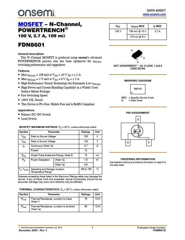
DATA SHEET www.onsemi.com
VD...