FDB2552 / FDP2552
October 2002
FDB2552 / FDP2552
N-Channel PowerTrench® MOSFET 150V, 37A, 36mΩ
Features
• r DS(ON) = 3...
FDB2552 / FDP2552
October 2002
FDB2552 / FDP2552
N-Channel PowerTrench®
MOSFET 150V, 37A, 36mΩ
Features
r DS(ON) = 32mΩ (Typ.), VGS = 10V, ID = 16A Qg(tot) = 39nC (Typ.), VGS = 10V Low Miller Charge Low QRR Body Diode UIS Capability (Single Pulse and Repetitive Pulse) Qualified to AEC Q101
Formerly developmental type 82869
Applications
DC/DC Converters and Off-line UPS Distributed Power Architectures and VRMs Primary Switch for 24V and 48V Systems High
Voltage Synchronous Rectifier Direct Injection / Diesel Injection Systems 42V Automotive Load Control Electronic Valve Train Systems
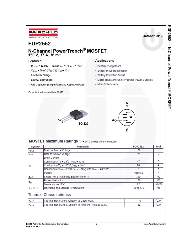
D
DRAIN (FLANGE) SOURCE DRAIN GATE SOURCE GATE
G
TO-220AB
FDP SERIES
TO-263AB
FDB SERIES
DRAIN (FLANGE)
S
MOSFET Maximum Ratings TC = 25°C unless otherwise noted
Symbol VDSS VGS Parameter Drain to Source
Voltage Gate to Source
Voltage Drain Current Continuous (TC = 25oC, VGS = 10V) ID Continuous (TC = 100oC, VGS = 10V) Continuous (Tamb = 25oC, VGS = 10V) with Rθ JA = 43oC/W Pulsed EAS PD TJ, TSTG Single Pulse Avalanche Energy (Note 1) Power dissipation Derate above 25oC Operating and Storage Temperature 37 26 5 Figure 4 390 150 1.0 -55 to 175 A A A A mJ W W/oC
o
Ratings 150 ±20
Units V V
C
Thermal Characteristics
Rθ JC Rθ JA Rθ JA Thermal Resistance Junction to Case TO-220, TO-263 Thermal Resistance Junction to Ambient TO-220, TO-263 (Note 2) Thermal Resistance Junction to Ambient TO-263, 1in2 copper pad area 1.0 62 43
oC/W o o
C/W C/W
This product has bee...